PnP data is usually generated by the CAD system used to design the PCB. If PnP data is not available, it can be created manually.
Typically, PnP data consists of four, five or six values per component:
- Designator
- X position (typically in mm, inch or mil)
- Y position (same unit of measure)
- Rotation in degrees (usually counter-clockwise)
- Description (perhaps in several columns)
- Side (top or bottom; bottom sometimes called mirrored)
Click on the Import button in the Pick and place actions toolbar to select a PnP file for import. Alternatively, click on the small down-arrow in the lower right corner of the button to import a file which is already attached to the product.
Some CAD systems generate separate top and bottom PnP files. In this case, use the Bottom button to import the bottom side PnP file.
Macaos automatically imports several PnP formats. For those which are not recognized, or which have some level of ambiguity, the Pick and Place Data Import dialog box helps to specify how the data should be interpreted for import.
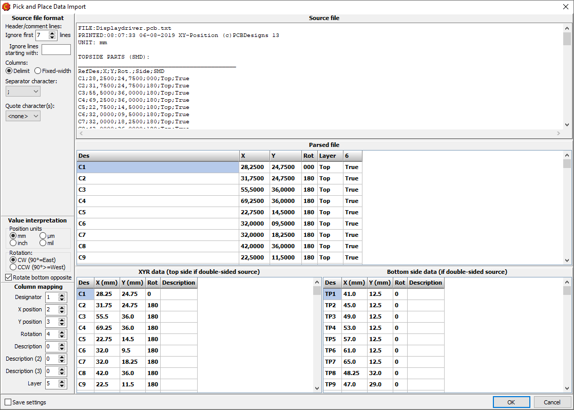
- If necessary, the source content may be edited, either directly in the text of the source file, or in individual cells of the parsed file.
- If necessary, specify the number of header rows to ignore, and the prefix character for comment lines.
- Specify whether the input file has delimited or fixed-width columns. For delimited columns, specify the delimiter character (and quotation character, if necessary). For fixed-width columns, specify the column widths.
- Specify the unit of measure used for X and Y coordinates. If incorrectly specified, the scale of the component layer will not match the scale of the PCB.
- Specify whether rotations are clockwise or counter-clockwise. Normally, bottom side component rotations should be imported in the opposite direction. If this doesn’t work with your file format, remove the check mark from Rotate bottom opposite.
- Normally, bottom side rotations are flipped horizontally (around the Y-axis). For PnP files which flip the rotation vertically (around the X-axis), such as those from Altium, set a check mark at Flip bottom vertically.
- Specify the input column numbers for each output field.
If there are components that might need further attention after import, set a check mark by each of them. This will create a component alert, and the component will be highlighted with red text in the component list. Note: Component alerts are not saved with the product. You should resolve all alerts before closing the ADM.
Once the data format has been correctly specified, click the OK button to import the data.
If necessary, align the component layer with the PCB.
Fiducial marks
Most Pick and Place systems expect there to be three fiducial marks on the board, typically near each of three corners. The locations of these fiducial marks need to be included in the PnP data.
If the board does not have dedicated fiducial marks, other optically distinct features, such as through-hole pads, may be used. Note: Via holes covered with solder mask are usually not suitable as fiducial marks.
- Left-click and draw a rectangle around the pad to use as a fiducial mark.
- The fiducial mark is added at the center of the selected pad.
Note: If a pad (from the originally imported Gerber data) is drawn (as one or more wide lines/arcs) rather than flashed (as a single shape object) then it will not be identified as a pad in the above procedure. In cases where no pads are found within the selection rectangle, the (center of the) selection rectangle is used.
Creating PnP data manually
If PnP data is not available for a component, it may be created manually, as follows:
- If a similar component already exists, select it in the component list to copy its properties to the new component.
- Left-click and draw a rectangle around all pads of the component to create.
- Specify the component designator and (if desired) specify that component properties should be copied from the selected component. The new component designator must be unique.
- The component is added at the center of the selected pads.
Tip: Import BOM data prior to creating components manually. Components found in the BOM data which do not exist in the PnP data are automatically created and placed to the left of the PCB. They may then be moved to their correct position.
Note: If a component pad (from the originally imported Gerber data) is drawn (as one or more wide lines/arcs) rather than flashed (as a single shape object) then it will not be identified as a pad in the above procedure. In cases where no pads are found within the selection rectangle, the (center of the) selection rectangle is used.