The Assembly Data Manager (ADM) is an integrated BOM Tool and Pick and Place Data Manager for PCBs. It provides an environment for managing and reviewing Pick and Place (PnP) and Bill of Materials (BOM) data.
An integrated, standards-based solution
The ADM helps dramatically reduce time and effort in preparing assembly data, by combining the following features in a single module:
- Graphic viewer with component editing functionality
- Structured component overview with properties editor
- Component search facility
- Send RFQ for assembly to participating EMS providers (Enterprise Basic version only)
- Component rotation, height and solder temperature editor
- Component price estimator (EMS version only)
- Export PnP and BOM data (EMS version only)
The ADM makes use of the Gerber Format X3 extensions1 to combine PnP, BOM and Assembly Drawing data into an integrated component layer of a PCB product. As CAD systems2 implement these extensions, a rapid and error-resistant path from designer to manufacturer may be achieved.
The component layer displays the location, rotation, size and key pin location of each component together with properties such as manufacturer part number, supplier SKUs, height, max solder temperature, etc. The use of a standards-based structure for this information allows purchasers, supplers, process line operators, etc to automate their systems and thereby reduce costs.
Including test points in your imported PnP data (or defining them in the ADM) makes them available to the Test Fixture Designer. Components with a TPxx designator are automatically assigned to the Test Point component class and marked as Do Not Place during import. The Test Fixture Designer will import each Test Point component and create a corresponding test pin. Note: For best results, all test points should be on the same side of the PCB.
1 Macaos actively participates in the development of these standards.
2 Some CAD systems, such as kicad, already support Gerber X3 output.
An efficient and straightforward workflow
- Import PnP data. (This may already have been done when the PCB product was imported.) This should be done prior to importing BOM data.
- If necessary, align the PnP data with the PCB data.
- Import BOM data. (This may already have been done when the PCB product was imported.)
- If necessary, move new components to their correct position. BOM components are matched to PnP components by their designators. BOM components which are not found in the PnP data are placed to the left of the PCB. Each of these should be moved to its correct position on the PCB.
-
If available, import test pad data in IPC-D-356 format. (This may already have been done when the PCB product was imported.) If necessary, align the test pad data with the PCB.
-
If test pad data exists, run the Merge action to extract key pins and footprint outlines from the test pad data.
- Draw outlines and mark Key Pins. For assembly purposes, it is desirable to graphically display the size and orientation of each component. This information is typically not included in the imported PnP or BOM data, but it can easily be added by drawing outlines and marking key (1 or A1) pins.
- Check/edit the properties of each component. Ideally, a complete manufacturer part number should be specified for each component. At the minimum, each component description should be unambiguous. The edit module includes an online component search function (powered by Octopart) to aid in quickly specifying unambiguous manufacturer part numbers.
- Save changes to the product and generate reports as desired.
Component List
The component list has three levels. At each level, two icons show whether or not the BOM and Placement status of the components has been checked and approved.
- The component class (resistor, capacitor, connector, etc).
The green icon indicates that the BOM status has been approved for all components in the class.
The blue icon indicates that the Placement status has been approved for all instances in the class. - The component (a single part number). When editing a component, you can change the properties which apply to all instances of that component.
The green icon indicates that the BOM status has of the component been approved.
The blue icon indicates that the Placement status has been approved for all component instances. - The component instance (at a specific location). When editing a component instance, you can change the rotation and placement status of that instance.
The blue icon indicates that the Placement status has been approved for the component instance.
The other icon which indicates whether the component is a fiducial mark, should not be installed, is a PnP component or is a non-PnP component. The icon also indicates whether the component is on the top or bottom layer.
Clicking on a component or instance displays its properties in the component editor. Double-clicking also zooms the viewer to the component. Right-click on the component list to specify the zoom size. You can also press Ctrl+Z to zoom to the selected component/instance, Ctrl+E to edit the selected component/instance or Ctrl+D to edit and open the online search module.
Note: If two or more component instances are grouped together, even though they should not be, this can be corrected by changing the Manufacturer Part Number of the instance(s) to be removed from the group. To do so, select the instances to be modified, right-click and select Change part number of instance and then enter the correct part number.
Clicking on the Highlight instance button zooms the viewer to the selected component and highlights it with three concentric circles. Clicking on the Highlight all instances button zooms the viewer to all instances (on the same side) as the selected component and highlights each of them with three concentric circles. If Highlight instance pads is checked, then all of the component’s pads will also be highlighted. Note: Highlighting pads is not supported unless IPC-D-356 data has been imported.
To search for a component in the list, type the designator in the text box at the bottom of the component list. It is also possible to enter a range of designators, such as C13-C25. The tree buttons may be used to expand or collapse the component list. The Exclude from list buttons may be used to hide components which are approved or have a specific placement status.
Component Alerts
A component alert indicates that the component needs further attention. When importing PnP or BOM data, setting the check mark for a component creates a component alert. These components have red text in the first column of the component list. Right-click on a component instance (or press Alt+A) to toggle the alert status of the selected components. Note: Component alerts are not saved with the product. You should resolve all alerts before closing the ADM.
Component display
Graphically, how a component displays depends on how much information about the component has been specified. At the minimum, a 0.3 mm circle is drawn at the component’s location (centroid/pick point).
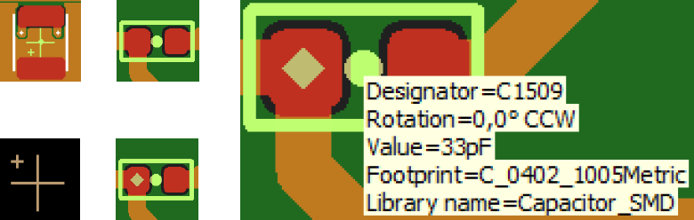
- If only the component’s location and rotation are specified (typically if imported from PnP data), then the component is displayed as a 20-pixel cross with a 5-pixel cross toward the unrotated component’s upper left corner. In other words, if the component rotation is 90 degrees, then the 5-pixel cross will be in the lower left corner. The cross symbols are always 20 and 5 pixels, regardless of zoom factor. Note: The 0.3 mm circle is not drawn when the zoom factor is so high that it would hide the 5-pixel cross.
- Components where the location is not specified (typically if imported from BOM data) are placed to the left of the PCB, with 10 mm spacing.
- If the component outline has been specified, then the outline is drawn with a 0.1 mm line. In this case, no 20-pixel cross is shown.
- If the location of the key pin (typically pin 1 or A1) is specified, then a 0.36 mm diamond is drawn at the location of the key pin. In this case, no 5-pixel cross is shown.
Press the Ctrl key and hold down the left mouse button on a component to view component properties such as designator, rotation, value, manufacturer part number, etc.
Press the Ctrl and Alt keys and click a component to locate it in the Component list.
Component rotation
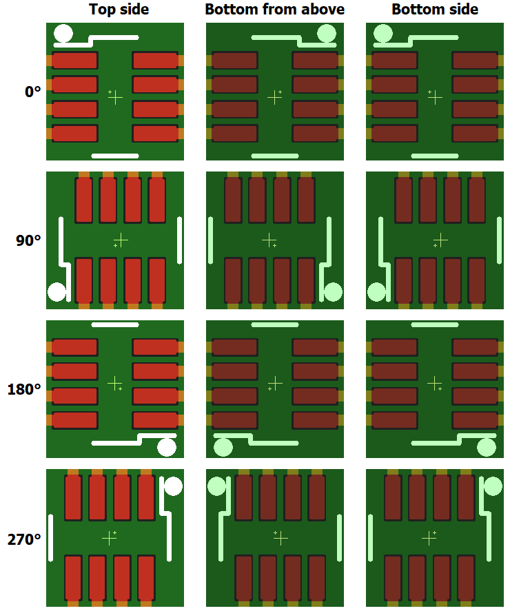
A component’s rotation specifies how the component is rotated from it’s nominal position when placed on the PCB. IPC-7351 specifies the nominal, or 0°, rotation as follows:
- For two-lead components, the key pin is (pin 1, + or cathode) is at the left
- For components where the key pin (1 or A1) is near a corner, that corner is at the upper left
- For components where the key pin is at the center of a side, the key pin is at top center
If the component is placed on the bottom side of the PCB, then the above rules apply as if viewed from the bottom side. This means that when viewed from the top side, the component is mirrored along the X-axis (left/right swapped).
Rotations are always specified as counter-clockwise. However, due to the mirroring, when viewed from the top side, components on the bottom will appear to be rotated clockwise.
The image to the right shows how bottom side components will appear when viewed from the top side (middle column) and when viewed from the bottom side (right column).
Graphic operations
A number of graphic operations are available: