-
Placement: PTH components should, to the extent possible, be placed together. They should be placed far enough from solder-side SMT components to meet the clearance and aspect ratio requirements shown below.
Long PTH components should be placed parallel to the direction of travel over the solder wave. Allow space between long components to close the opening in the solder pallet, in order to increase the strength and functionality of the seal wall and pallet floor.
Do not place SMT components within PTH land patterns. Avoid placing taller SMT components close to PTH components.
-
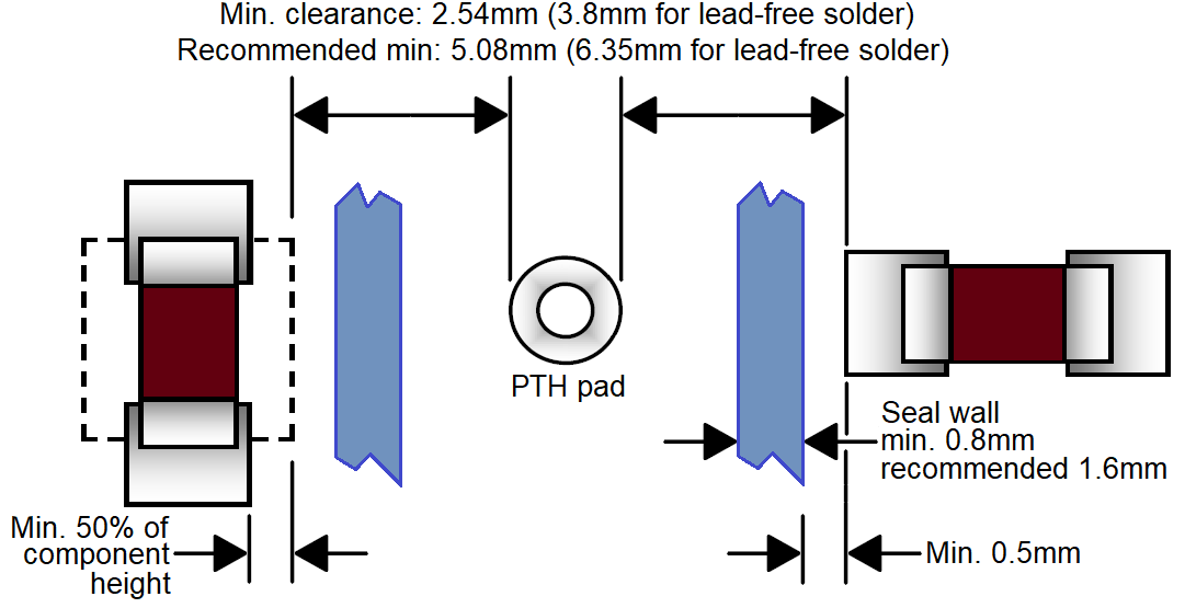 Clearance: In order to insure sufficient space for the solder wave to adequately solder the plated through-hole, the clearance between PTH pads and SMT pads must meet the minimums shown here. Note that lead-free solder waves require a larger clearance.
 -
Aspect ratio: Openings in the wave solder pallet must be large enough for the wave to enter with sufficient pressure to apply solder. Placing taller SMT components farther away from the opening, allows the pallet floor to be “lifted,” thereby improving solder wave pressure.
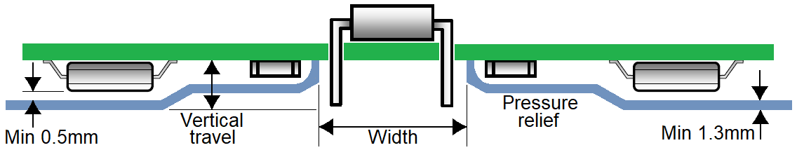
The aspect ratio is defined as opening width / vertical travel, where the width is the dimension perpendicular to the direction of travel. For PbSn soldering, the minimum aspect ratio is 1.0 while for lead-free soldering it is 1.7, as shown in the table below.
Vertical travel SnPb solder Pb-free solder ≤3.8 mm 3.8 mm 6.35 mm 5 mm 5 mm 8.5 mm 6 mm 6 mm 10.2 mm 7 mm 7 mm 11.9 mm 8.15 mm 8.15 mm 13.85 mm The minimum opening width is 3.8 mm for PbSn soldering and 6.35 mm for lead-free soldering, even if the vertical travel is less than 3.8 mm.
If the opening width is less than 7.6 mm then the opening length (parallel to direction of travel) should be at least 3 times the width. For larger widths, the length should be at least as large as the width.
-
Vertical travel: The minimum clearance between the PCB/components and the pallet floor is 0.5 mm. The minimum floor thickness is 1.3 mm. The maximum allowed vertical travel is 8.15 mm, giving a maximum component height of 6.35 mm.