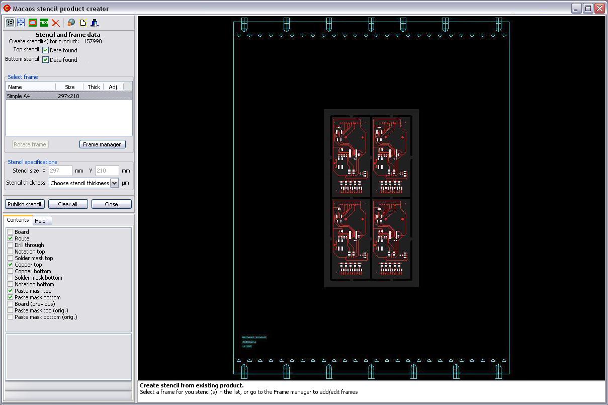
Macaos has developed a powerful and flexible tool for designing solder paste stencils from your PCB data.
Using the copper layer and paste mask layer data from the PCB, you can do the following:
- Select a frame from among pre-defined or uploaded frame data
- Adjust all opening sizes by a percentage of area
- Adjust the corner rounding of all openings
- Fine tune individual opening sizes to correct for process issues
- Mark fiducials for etching (rather than cutting)
- Add text
- Place top and bottom openings side by side on the same stencil
- Split a large opening into an array of smaller openings
- Define "step" regions of the stencil to be etched down to a different thickness
All opening size adjustments are defined as a percentage of the copper pad area (when copper data is available). The WYSIWYG viewer lets you see how your adjusted openings compare to the copper pads.
A frame manager and editor allows you to upload frames or build new frames based on pre-defined templates. Frames may be defined with variable texts (company name, product number, etc) which automatically get substituted in the Stencil Product Creator.


