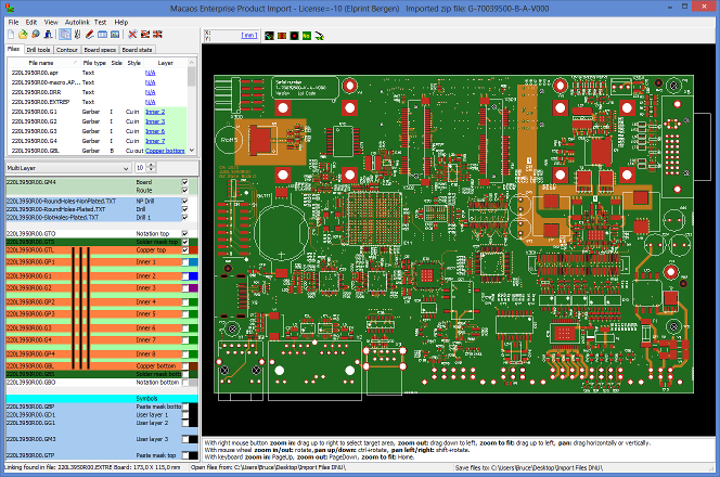
The Import Module is used to read Gerber and drill files or ODB++ data, as well as pick & place data and documentation, into the system and "package" the data into a PCB product. Each input file is automatically mapped to it's board layer, based on an AI-based filename analysis or by using pre-defined or customizable filename filters. A WYSIWYG viewer shows your board just as it will be interpreted by the manufacturer. Once the PCB has been saved as a MIF file, it is ready for panelization and other operations.
Stackups
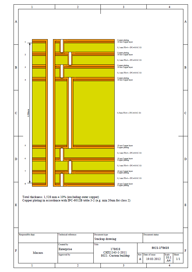
When defining your board, you may choose from a large selection of pre-defined stackups, or define your own buildup. Either way, a high quality technical drawing of the stackup is automatically generated in PDF format.
The custom stackup editor supports flexible, flex-rigid and metal-based stackups. The most common material types (defined by IPC-4xxx slash sheets) are available for selection. If desired, you may query the CircuitData materials database when specifying dielectric materials for special needs.
Symbols

A unique feature of the import module is the ability to add symbols or fiducial marks to the component legend or solder mask layers. Available symbols include: Lead-free, CE-mark, WEEE, Recycle, ESD, RoHS, text, bar code, fiducial and the fabricator's UL-mark.
There is also a function to generate an IPC/JEDEC J-STD-609A compliant text string specifying the materials used in the PCB.