What was new in Macaos Gallery
What was new in Macaos Gallery
Macaos Gallery 2.6 (September 2021)
Macaos Gallery 2.6 (September 2021)
IPC-D-356 Test Pad Data
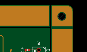
With this release, we add support for bare-board test pad data. Most CAD systems are able to generate test pad data in IPC-D-356 format. Including this data together with your Gerber and Drill files is not just an advantage for the manufacturer when testing bare PCBs, but it also makes several operations in Macaos Enterprise quicker and easier.
- Import module: If an IPC-D-356 file is included in the batch of files to be imported, it will be automatically detected, imported and linked to the Test pad top and Test pad bottom layers. Each testable point (typically bare copper pads and plated holes) is imported together with its designator, pin number and net name. If necessary, the test pad layers may easily be aligned with the Gerber layers.
- Assembly data manager (EMS version only): If test pad data was not imported at the time the product was created, it may be added to the product in the ADM. A Merge function matches test pad data to the product's components, automatically identifying component footprint outlines and key pins, where possible.
- Test fixture designer (EMS version only): When creating a test pin, if a test pad exists at that point, then the designator, pin number and signal name will be copied from the test pad.
- Solder paste stencil creator: When test pad data is available, then it is possible to match stencil openings to component footprints. The footprint editor can easily modify all shapes in a footprint symmetrically. This can also be done in a single operation on all components having the same footprint.
Assembly Data Manager improvements (EMS version only)
In addition to adding support for test pad data, we have made additional tweaks to streamline ADM usability. Our goal is to make the process of verifying PnP and BOM data as quick and painless as possible. Here's a list of the tweaks:
- Ctrl+Alt+Click on a component in the viewer to locate that component in the component list
- Right-click on a component instance and select Change part number of instance to edit the manufacturer part number of that instance. This function is intended for use if an instance inadvertently gets grouped together with other non-matching components.
- Component alerts: In the PnP and BOM import dialog boxes, there are now check boxes in the component lists. Setting a check mark causes that component instance to be flagged with an "Alert." After import, the flagged components will show with bold red text in the component list. Right-click on a component instance to toggle the alert on or off.
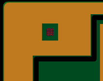
- We have added buttons at the bottom of the Component Properties pane to highlight the selected component instance, or all instances of the selected component. If test pad data is available, then the instance's pads may also be highlighted.
- In the component search dialog box, we have added check boxes to the search results list, which are used for selecting the manufacturer part number and alternates.
- In the component search dialog box, we have added an additional search text field.
- When importing a BOM, if marking capacitors or resistors as Equivalent or better, it is now possible to specify individual components (by designator) which should not be marked.
Other improvements
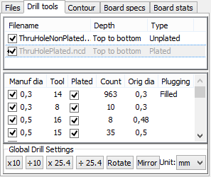
- Import module: You can now right-click on a drill file (in the drill files list) to toggle all tools in the file between plated and non-plated.
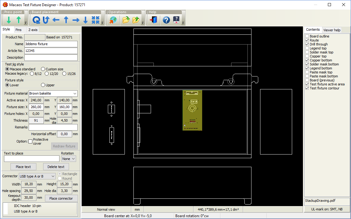
- Test fixture designer (EMS version only): We have added Test fixture drawing and Test fixture annotation layers to improve fixture documentation. The Test fixture drawing layer shows all test pins with a symbol (for the receptacle size) and a text (for the pin head style, if specified). Guide pins are shown with a large cross and a letter indicating the pin function. The Test fixture annotation layer shows all test pins with a cross and a text with the Des-Pin of the test pin (if specified).
- Test fixture designer: It is now possible to export the test circuitry PCB in DXF format.
Macaos Gallery 2.5 (June 2021)
Macaos Gallery 2.5 (June 2021)
Macaos Gallery 2.5
Test Fixture improvements
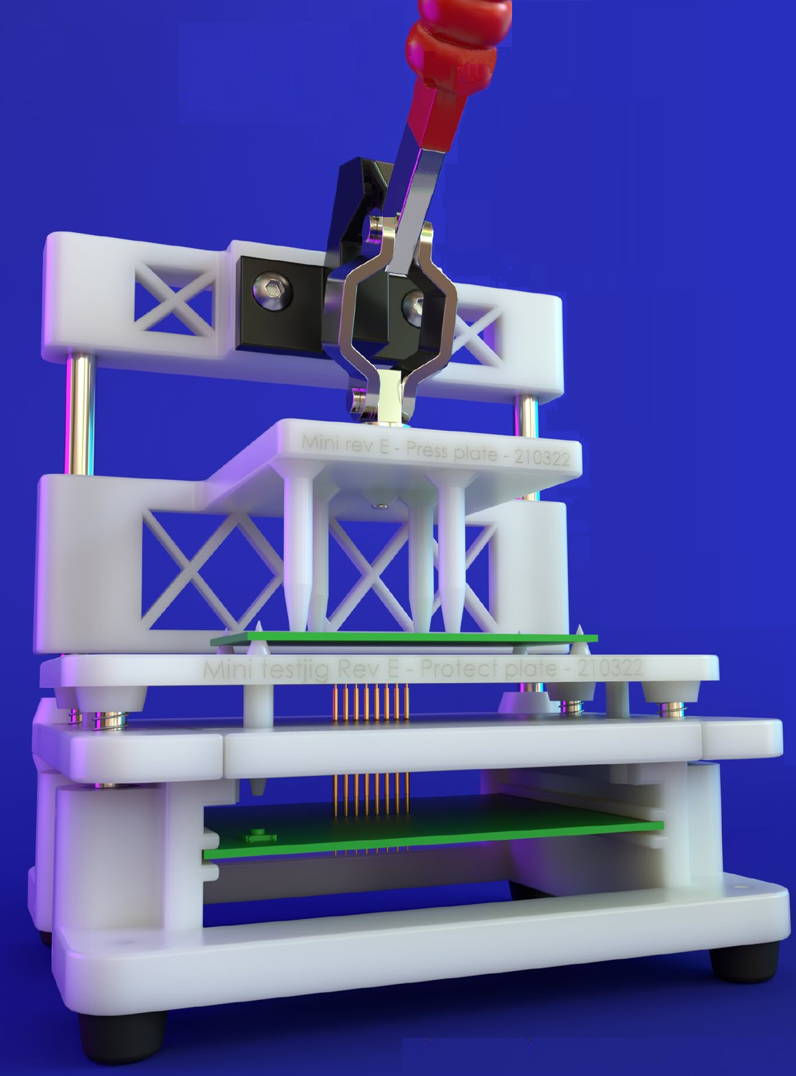
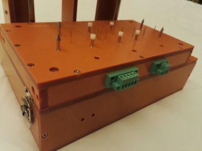
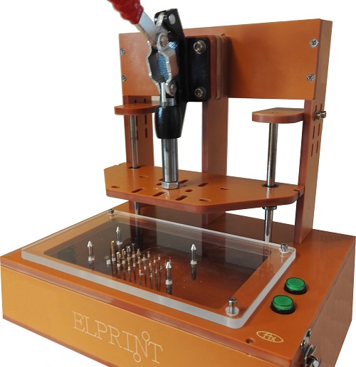
Macaos Integrated Test Jig
The test fixture designer module now supports design of the Macaos Integrated Test Jig, a new design which integrates test circuitry into a modular test jig. It is developed for increased reliability and ease of design, compared to other supported test jigs.
The Macaos Integrated Test Jig incorporates an upper press fixture, a protective cover, a receptacle plate, and a test circuitry PCB. This is delivered fully assembled, with pins/receptacles installed.
The user selects an active area size, and then specifies the locations and types of Guide Pins and Test Pins. From this information, the Upper Fixture, Protective Cover and Receptacle Plate (the three gray modules shown at the right) are generated and added to the jig.
Use the Gerber button to generate a Gerber file of the test circuitry PCB outline and pin locations, for import to your CAD system. Connectors and indicators may be placed at the front and/or back edge of the PCB. This PCB must be ordered together with the test jig.
Automatic test pin placement
Test points that have been defined in the Assembly Data Manager (with the Test Point component class) may be automatically imported as test pins. The user need only specify a receptacle size (diameter) and pin head style.
Other tweaks
When publishing a test fixture, it is now possible to attach a STEP file (3D model) of the PCBA to be tested. This is strongly recommended when publishing a Macaos Integrated Test Jig.
As test pins are added to the fixture, the centroid of the test pins is shown as a hexagon.
Assembly Data Manager improvements
We have made additional tweaks to streamline ADM usability. Our goal is to make the process of verifying PnP and BOM data as quick and painless as possible. Here's a list of the tweaks:
BOM Import
- If designators are separated by a comma, semicolon, or space, the separator character will be automatically identified in most cases.
- An option has been added to treat the hyphen (-) as a valid designator character, instead of treating as a designator range character.
- Up to three Value columns (in the source grid) may be specified.
- If desired, all capacitors and/or resistors may be marked as "equivalent or better" during import.
- Right-click on a column to search and replace text in the selected column.
- A button has been added to clear all BOM import configuration settings.
Other tweaks
- The shortcut key for opening the component search dialog has been changed from Ctrl+O to Ctrl+D in order to make it easier to use with only the left hand.
- Additional commands have been added to the right-click menu of the component tree, to remove approval state, remove alternate manufacturer part numbers, and more.
Macaos Gallery 2.4 (February 2021)
Macaos Gallery 2.4 (February 2021)
Panel module improvements
Panel scripts
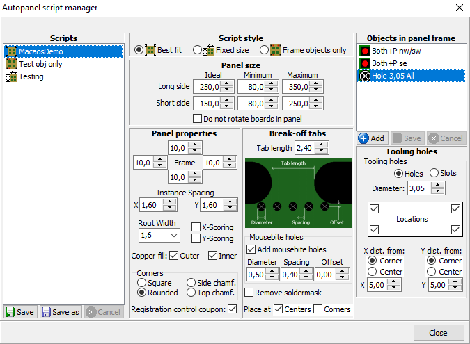
The panel script feature has been expanded to support fixed size frames, as well as scripts which only add frame objects to an existing panel. If desired, board rotation in a best fit script may be disabled.
It is now also possible to add text or a bar code to a panel script. You may specify any text, or right-click on the text field to insert the product number, name, article number, description or date of panelization.
 Add board as a test coupon
Any (small) board may be added to the panel frame as a coupon. (When selecting a board, a warning is shown if the board appears to be too large for the frame.) For each layer in the panel, data from the board is copied to the desired location in the frame.
Other tweaks
A notch may be added to the panel frame by placing a tooling hole or slot at the edge of the frame.
Diamond and octagon have been added to the available shapes for fiducial marks.
When placing an impedance coupon, if the frame width is too small for the coupon you may choose to automatically enlarge the width of one or more frame sides to accommodate the coupon width.
Import module improvements
When importing an archive which contains both Gerber/Drill and ODB++ data, the user may choose which dataset to import. (The other dataset will be ignored.)
Layers have been added for Beveled edge, Coating top and Coating bottom.
It is now possible to mark drill tools as countersink. This is done in the same manner as for marking drill tools with via protection or as press-fit holes.
Assembly Data Manager improvements
Note: The ADM is only available in Macaos Gallery EMS version.
We have made numerous tweaks to streamline ADM usability. Our goal is to make the process of verifying PnP and BOM data as quick and painless as possible. Here's a list of the tweaks:
ADM module
- New shortcut keys: Ctrl+Z=zoom to component; Ctrl+E=enter edit mode; Ctrl+S=save and exit edit mode
- Ctrl+Click on component in viewer (to see component properties) works when in Move mode (but not other graphic modes)
- BOM Placement list sorted in same order as component tree
- Added Viewer button beside BOM list buttons in toolbar
Add component/Add fiducial
- When adding a component, you may copy properties from the component selected in the component tree
- Warn if specified designator is a duplicate and show alternatives
- After adding a component or fiducial, the module remains in add component or add fiducial mode
- Does not reload view if focused component's layer is already visible
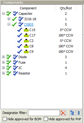 Component tree
- Filter list by designator
- "All approved" icons at parent level(s)
- Value or OrigDescr is shown in the tooltip of Component level items
- Hide approved components
- Buttons to expand or collapse all levels of tree
- Added Mechanical, Fuse, and Crystal component styles
- Set Equivalent or Better for selected components
- Set or remove Include in PnP Output for selected components
- Set zoom size for double-click on component
Component editor
- Check box for Allow Equivalent or Better
Import BOM
- Add column to source grid
- Edit text in selected cells (both grids)
- Edit text in all cells of selected column (both grids)
- Specify default mounting style when no column mapped for mounting style
Other improvements
A major change in this release is under the hood. We have increased the resolution of our internal database from 100 nm to 1 nm. Among other things, this will greatly reduce round-off errors in determining the center of arc objects.
Viewer: When measuring, the angle from start to end point is also displayed.
Macaos Gallery 2.3 (October 2020)
Macaos Gallery 2.3 (October 2020)
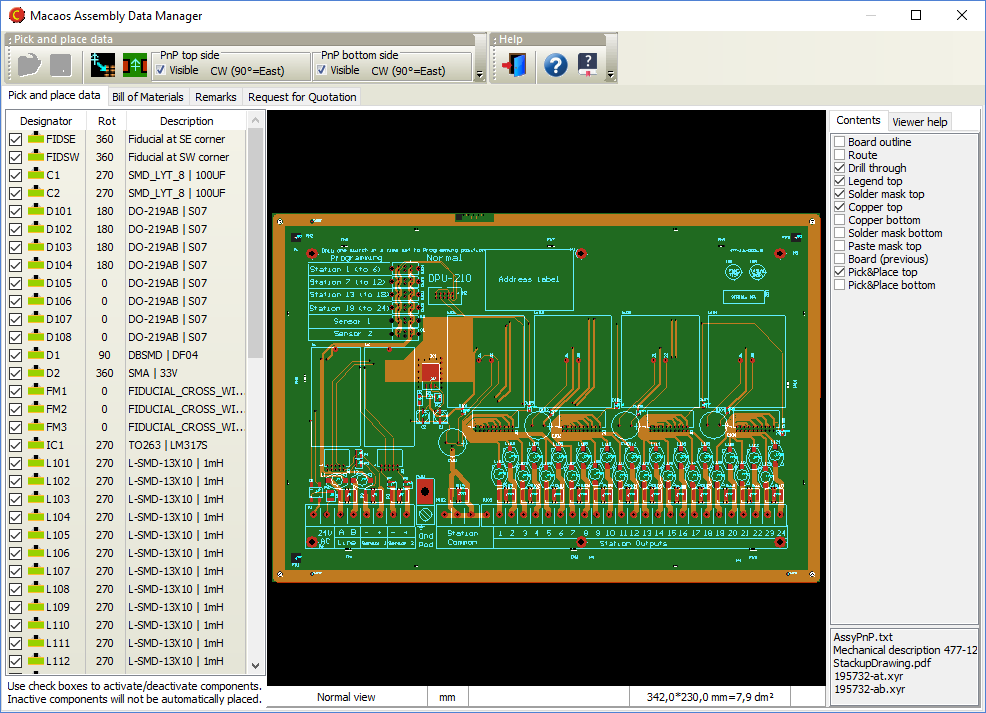
Assembly Data Manager (ADM)
The new Macaos ADM is an integrated BOM Tool and Pick and Place Data Manager for PCBs. It provides an environment for managing and reviewing Pick and Place (PnP) and Bill of Materials (BOM) data.
Note: This module is only available in the EMS version of Macaos Gallery.
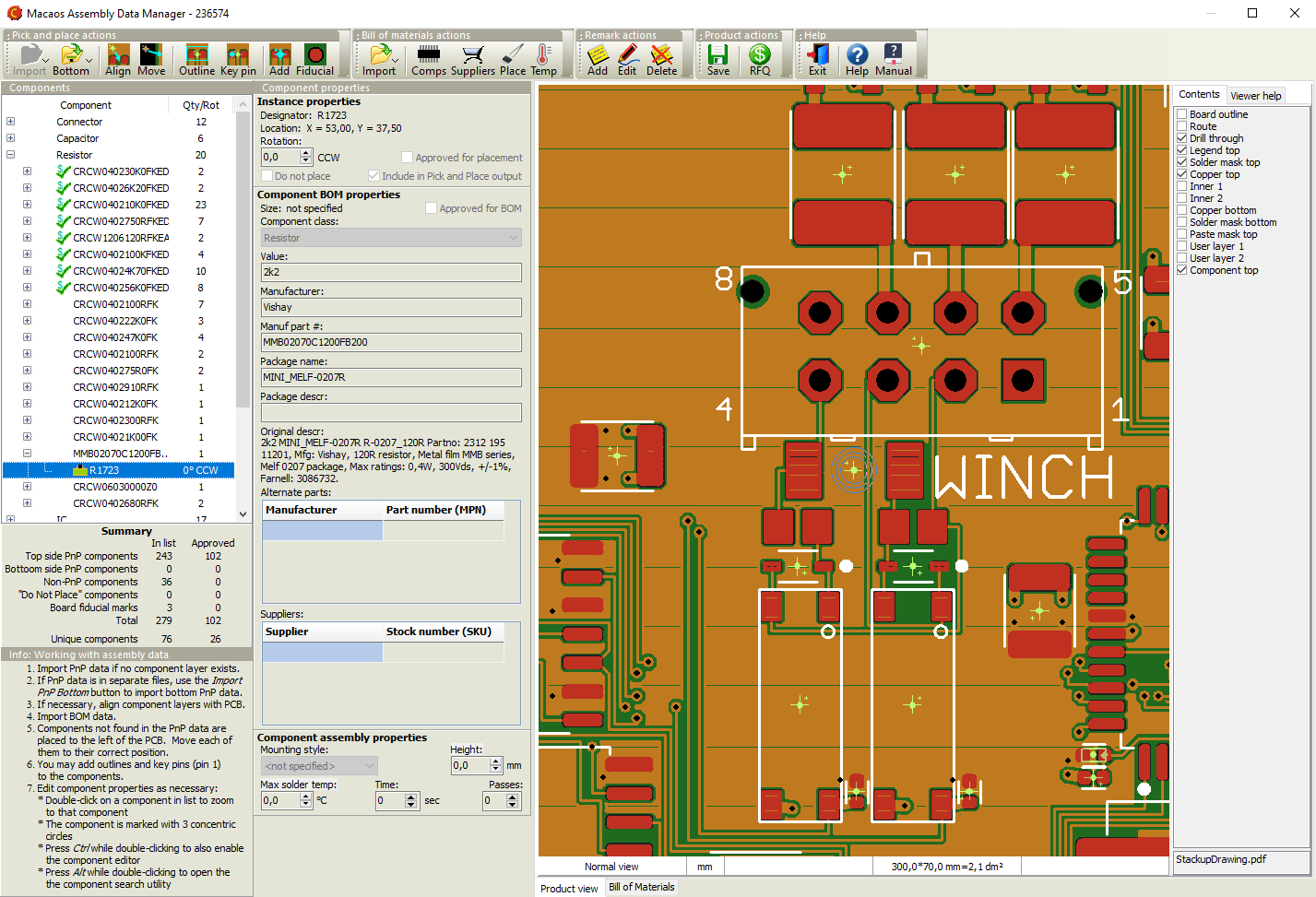
The ADM helps dramatically reduce time and effort in preparing assembly data, by combining the following features in a single module:
- Graphic viewer with component editing functionality
- Structured component overview with properties editor
- Component search facility
- Component price estimator
- Component rotation, height and solder temperature editor
- Export PnP and BOM data
The ADM makes use of the recently released X3 extensions1 to the Gerber Format to combine PnP, BOM and Assembly Drawing data into an integrated component layer of a PCB product. As CAD systems2 implement these extensions, a rapid and error-resistant path from designer to manufacturer may be achieved.
The component layer displays the location, rotation, size and key pin location of each component together with properties such as manufacturer part number, supplier SKUs, height, max solder temperature, etc. The use of a standards-based structure for this information allows purchasers, supplers, process line operators, etc to automate their systems and thereby reduce costs.
1 Macaos actively participates in the development of these standards.
2 Some CAD systems, such as kicad, already support Gerber X3 output.
See the ADM user guide for more info.
Note: The ADM is not included with Macaos Gallery Pro.
Simple PCB Editor
With the Simple PCB Editor, it is possible to make certain adjustments to a PCB product. You can:
- Change the diameter of a contour tool or drill tool
- Toggle the plating of a drill tool’s holes
- Change the extent (depth) of a drill layer
- Reassign (swap) or change the polarity of copper layers
- Change the via protection style of a via protection layer
- Replace a layer with the contents of a Gerber file
Right-click on a single-board PCB product (in the Product Browser) to open the Simple PCB Editor.
Stencil module improvements
The stencil module now calculates the Aspect ratio and Area ratio for the smallest apertures in the stencil. This is used to recommend a maximum stencil thickness when creating a stencil. See Stencil ratios for more info.
DXF file import
Limited support for importing DXF files has been added. A DXF file may be imported to a user layer in the Import module. When loading a file directly in the Stencil module, you may load either a Gerber file or a DXF file.
Only those DXF entities which easily map to Gerber-style objects are imported. Other entities are ignored. For more info see DXF Files.
Other improvements
The biggest change in this release is under the hood. We have enhanced our Gerber reader and writer to be fully compliant with all features of the latest Gerber Format standards. This improves data reliability from your CAD system all the way to the manufacturing processes.
Macaos Gallery 2.2 (December 2019)
Macaos Gallery 2.2 (December 2019)
Create wave solder pallets
With this new module, you can quickly design a pallet for transporting a board or panel through a solder wave. Solder pallets are useful when working with small, thin or irregular boards, as well as with boards that have both PTH components and solder-side SMT components.
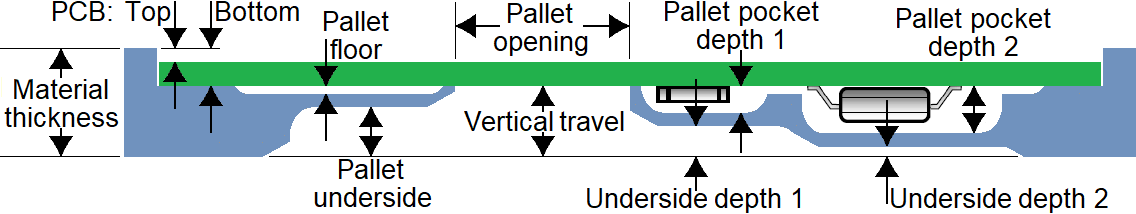
Two styles of pallets are supported:
- A wave solder pallet exposes the entire board to the solder wave.
- A selective wave solder pallet exposes only specified regions of the board to the solder wave.
Creating a selective wave solder pallet is easy:
- Select a material and thickness and specify component pocket depths.
- Place board fasteners at desired locations around the board.
- Draw "opening" outlines around the components to be soldered.
- Draw "pocket" outlines around the solder-side components that are covered by the pallet.
- Generate a milling file for the pallet.
All other elements of the pallet are calculated automatically. This includes edge rails, bottom side bevels, pallet floor, seal walls, etc.
Creating a wave solder pallet is even easier, since steps 3 and 4 above are unnecessary.
Note: Selective wave soldering requires some planning during board layout, in order to have sufficient clearance between wave-soldered components, and components which must be shielded from the solder wave.
PCB as test fixture
 The Test Fixture Designer module has been expanded to allow creating a PCB test fixture.
Rather than using a sheet of fixture material as a holder for the test pins, it may sometimes be more useful to mount the test pins directly into a PCB.
For a standard test jig, choose Lower w/ PCB. For other jigs, choose Lower - flat and set the thickness to 3.2.
Use the Gerber button to export the fixture outline and holes to a Gerber file, which may then be imported to your CAD system for further design.
Import module improvements
PnP format specifier dialog box
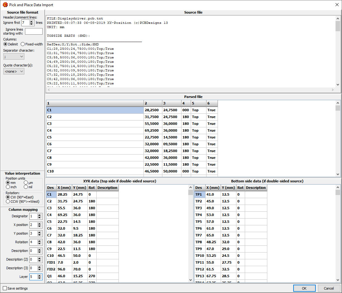
When importing a Pick and Place file, if the file format is not automatically recognized, you can specify the format as necessary.
Mark holes as press-fit
It is now possible to mark holes as press-fit. This is done by right-clicking on the appropriate tool(s) in the drill tool list, and selecting Via protection/Press-fit|Press-fit.
Laser cutter tool size for flex boards
For flex boards, it is possible to choose Laser as a cutter diameter. Note: Laser is only suitable for outer and inner contours.
Backdrill layers
Drill files may be assigned to backdrill layers.
Export improvements
Pick and Place format
It is now possible to specify the format of exported PnP data. You may choose between delimited or fixed-width columns and specify which field is mapped to which column. You may also select the unit of measure for X/Y coordinates and whether rotations should be clockwise or counter-clockwise. You may also specify a file header text, as well as the text to use for top/bottom sides if a layer column is exported.
Export profiles
Export profiles have been expanded to store all export settings in the profile. In addition to filename patterns, each profile now also includes drill file format, PnP format, inclusion of additional files, and Gerber X2 attributes
Other improvements
Configuring network paths
In the Macaos Gallery Options dialog box, it is now possible to right-click and enter a path (such as for the location of the Gallery Archive). This is useful for entering network paths which are not found in the folder chooser dialog box.
Stencil improvements
An operation has been added to the Transfer module which copies all toolinig holes from the panel frame to the stencil.
It is now possible to specify the size of text in stencil frames.
Pro version improvements
Support for shipment methods
The price engine has been expanded to add support for multiple shipment methods. See What's new in version 2.2 in the Pro Version Features user guide for a detailed explanation.
Seller's part number
In the Quotation details dialog box, it is now possible to specify the seller’s part number. This will show in the printed quotation (if supported by your quotation template).
Macaos Gallery 2.1 (February 2019)
Macaos Gallery 2.1 (February 2019)
New panel module featuresAllow rout slots to cross scoring linesNormally, rout slots end at scoring lines, in order to prevent notches in neighboring boards. This can lead to unwanted burrs or sharp corners at the routing/scoring interface. For symmetrical boards, the slot may cross the scoring line without entering the neighboring board. 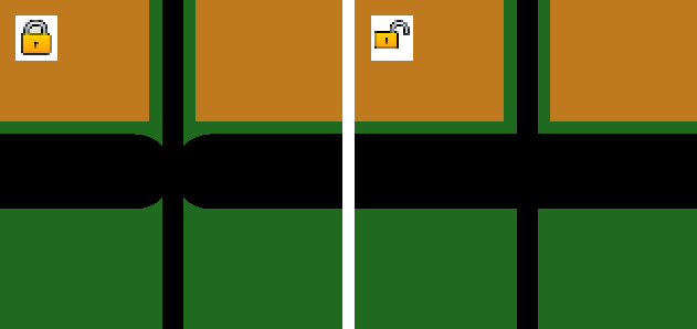
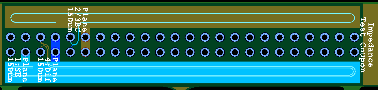
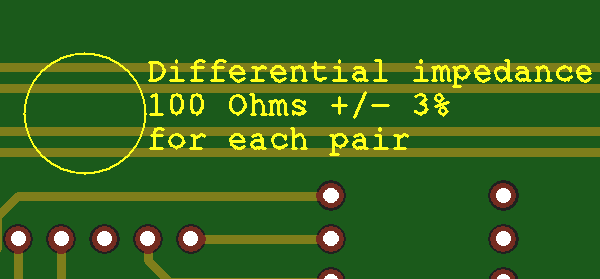
When scoring is enabled, a padlock is shown. Click on the padlock to "unlock" the routing/scoring interface. When scoring is "unlocked" then the routing slots extend one radius beyond the scoring line. It is the user's responsibility to insure that any notches which may arise within neighboring boards are acceptable. IPC-2221 Z-style Impedance test couponAn impedance test coupon may easily be added to the margin of a panel. The user need only specify the signal style, layer and trace width (and spacing). The coupon is then automatically generated according to the specifications for a Z-style test coupon in IPC-2221.
A test coupon may contain up to 12 signals, but no more than two signals on a layer. Single-ended striplines and microstrips, edge-coupled differential striplines, and edge-coupled or broadside-couple microstrips are supported. See the test coupons help page for more info. |
Export separate plated and unplated drill filesWhen exporting a product to Gerber, the through hole drill layer may contain both plated and unplated holes. The Gerber file for this layer indicates unplated holes with square "holes." The drill data is also exported as drill files, in XNC format. Separate XNC files are generated for plated and unplated through holes. |
MIF file historyStarting with this version, a file history is saved with the file. It is also possible to add your own comments to the file history. This may be useful for tracking revision changes. Right-click on a filename and choose MIF file history. |
Support for CircuitData languageThe CircuitData language is an open language for communicating PCB specifications, requirements and capabilities. Macaos Enterprise supports both reading and generating PCB product specifications in CircuitData JSON format. A CircuitData file may be exported by right-clicking on a PCB product and choosing Export to CircuitData. See www.circuitdata.org for more information about the CircuitData language. |
Pro version enhancementsDisable price listIn the Quotation module, right-click on a price list to disable the price list. A disabled price list will be inactive (unchecked) each time the Quotation module is opened. Import RFQ from Macaos EnterpriseWhen enabled, a Macaos Enterprise user may choose to send an RFQ to a Macaos Gallery Pro user. You will receive an e-mail containing the RFQ and product specifications (either as a .mif file or as a BoardSpecs.txt file) which can be opened in Macaos Gallery Pro. Note: You must subscribe to the Macaos RFQ service and have this feature enabled for each customer company from whom you wish to receive RFQs. Prices from CircuitData or Gerber Job fileA CircuitData (.cdjson) or Gerber Job file (.gbrjob) may be imported in the Quotation module, allowing you to get prices for a product without having imported the Gerber/Drill files to Macaos Gallery. |
Macaos Gallery 2.0 (November 2018)
Macaos Gallery 2.0 (November 2018)
DepanelizationDepanelization is the process of removing individual boards from a panel, after the boards have been populated with components. Traditionally, boards have been depanelized by breaking or cutting the the break-off tabs which hold the panel together. However, the mechanical forces (particularly bending) which can take place may weaken or damage the solder joints of fine-pitch SMT components near the board edges. This problem can be mitigated by using a milling machine to remove the break-off tabs. The Depanelizer module allows you to easily and quickly accomplish the two specific tasks required for depanelization by milling machine:
Note: The depanelization is not available for Macaos Gallery users located in the Nordic countries. |
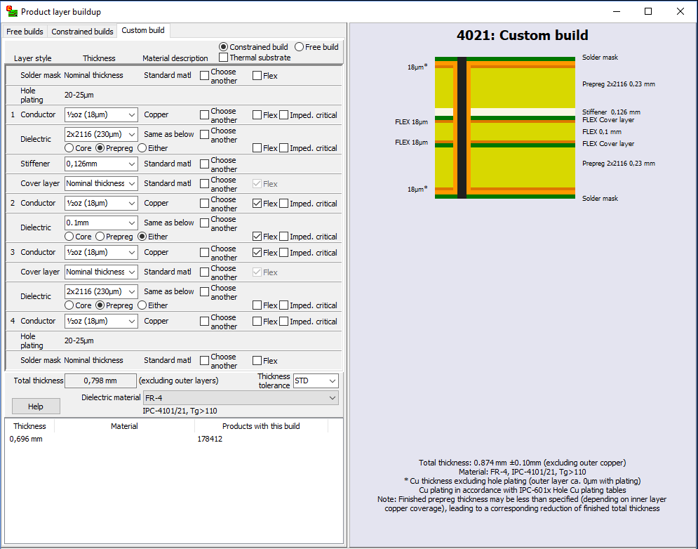
Stackups with odd number of layersIt is now possible to define a multi-layer custom buildup with an odd number of copper layers. For example, to define a 3-layer buildup, start by defining a 4-layer buildup. Then, choose Omit as the copper thickness of one of the inner layers. |
Panelization improvementsIt is now possible to specify the outer dimensions of a panel. In this way, you can adjust the width of the outer frame to give the desired total panel width/height. The outer dimensions may only be adjusted after the Panelize operation has been executed. It is now possible to place tooling holes and fiducial marks relative to the center of the panel. When specifying the X/Y distances, you can choose whether the distance is measured from the panel corner or the panel center. |
Other improvementsLook and feelWe've given all modules a new look. Modules now have a more consistent layout, with parameters at the top left, info/help text at the lower left, and the graphical viewer's layer list to the right. Button bars across the top of each module give quick access to the most commonly used functions. The graphical viewer has several status panels along the bottom edge, which display useful information. Click on the view mode or units panel to change the view mode or unit of measure. Automatic subfolder managementWhen theproduct archive contains many files (typically more than 1000-3000), then performance may become sluggish. If desired, Macaos Gallery can automatically organize your products into subfolders. Choose between numeric or alphanumeric subfolders. Numeric subfolder management creates a subfolder for each 1000 product numbers. Alphanumeric subfolder management creates subfolders for the first character(s) of the filename, automatically creating subfolders when the number of files in a folder exceeds a user-specified threshold. Gerber Job fileWhen exporting to Gerber, a Gerber Job file (.gbrjob) is included in the exported zip file. The Gerber Job file provides information which allows a manufacturer to automatically process the Gerber files and product properties. Export profilesIt is now possible to define multiple profiles for use when exporting a product to Gerber. For example, you could create a different profile for each PCB supplier you use. User-defined export profiles allow you to define the filename suffix and/or filename extension for each generated Gerber and Drill file. Check boxes allow individual files to be omitted from the output zip file. Minimum copper to unplated edge clearancePressing the N key (with the mouse over the graphic viewer module while viewing a PCB product), highlights and zooms to the objects having the minimum distance between a copper feature and an unplated hole or contour edge. Connection managerThe connection manager has been expanded with Ping and DNS lookup functions, which can help when troubleshooting connection issues. |
Macaos Gallery 1.7 (February 2018)
Macaos Gallery 1.7 (February 2018)
Import module improvements
Expanded custom stackup definition
In this version we have expanded the custom stackup definition module to better support flex and rigid-flex boards.
- In addition to the dielectric and copper layers which make up a stackup, it is now possible to define solder mask, cover layer, adhesive/bonding and stiffener layers.
Note: It is not necessary to add cover layer or solder mask layers to a simple stackup, since these layers are already specified by product properties. However, if you have special material or thickness requirements, or are defining a rigid-flex board, then these layers may be specified. - It is now possible to specify the thickness of dielectric and thermal substrate layers in a metal-based board stackup.
- Any individual layer may be marked as a flex layer. This would be used to indicate the layers in the flex region of a rigid-flex board.
Note: With this version you can define two stackup regions for a rigid-flex board: the rigid region (encompassing all layers) and an implied flex region (the layers marked as flex). Our goal is to support up to five stackup regions in the next major release of Macaos Enterprise. - The format for specifying stackup materials has been expanded. The material name and manufacturer may be specified, as well as whether or not the material must be halogen-free. For dielectrics, IPC-slash sheet and minimum Tg may also be specified.
Refresh file during import
If while preparing a product for import, you discover that a layer needs to be updated, you can replace that layer without having to restart the entire import process. Right-click on the file name and choose Replace file.
Note: It is not possible to replace the board/contour file. If this file needs to be updated then the entire product must be imported again.
Gerber job file
If the product you are importing contains a Gerber job file (*.gbrjob) then file linking information and product parameters will be extracted from the file.
Note: The final format of the Gerber job file has not yet been published. Some Gerber job files may not be compatible with the current draft specification. We will update this feature when the final format is published.
Macaos Gallery 1.6 (May 2017)
Macaos Gallery 1.6 (May 2017)
Replace board in panelA board may be replaced in a panel. To do so take the following steps:
|
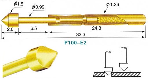
Test fixture improvements Macaos Standard JigThis version supports the Macaos standard test jig. The Macaos standard test jig is designed to use a lower fixture box with an internal height of 70mm, giving room for connectors, wiring and electronics in an easily swappable module. The Macaos standard jigs is supplied with an easily removable generic upper fixture allowing for flexible placement of press pins. An adjustment screw and magnet make it possible to finely adjust the spacing between upper and lower fixtures. Static guide pin placementIt is now possible to place static (non-deflecting) guide pins at any location along the edge of the PCB. Static guide pins are useful for insuring proper placement of boards that do not have holes with an appropriate diameter for normal guide pins. Specify or edit pin coordinatesIt is now possible to modify the pin coordinates and/or hole diameter when placing a test pin. It is also possible to edit these values after a pin has been placed. The coordinates and diameter of holes for guide/support/press pins may also be edited, by first right-clicking on the pin list and showing guide pins. View opposite test fixtureWhen creating a test fixture for the opposite side of an existing test fixture, the "other" test fixture may be viewed. Note: The "other" fixture data is not saved with the new fixture. |
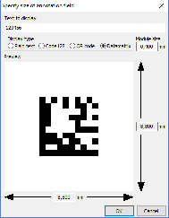
Annotation fields Annotation fields may be placed with an appropriate size for a text, bar code or 2-dimensional bar code. The Define annotation field dialog box automatically calculates the size of a rectangle for the text or bar code for a specified number of digits or alphanumeric characters, including appropriate margins. This feature is useful for laser marking of date codes and/or serial numbers. Annotation fields may be added to a new product in the Import module, or to a new panel in the Panel module. Annotation fields may also be added to an existing product with the Add Masks module. |
Other new featuresCancel symbol placementIn the Import Module, when drawing or placing a symbol, right-click to cancel the operation. |
Macaos Gallery 1.5 (February 2017)
Macaos Gallery 1.5 (February 2017)
Test fixture improvementsFixture specificationWhen creating a test fixture, you may choose a fixture suitable for one of the Macaos test jigs, or specify your own dimensions.
Macaos test jigs are supplied with a generic upper fixture allowing for flexible placement of press pins. In case of more specific needs, an upper fixture may be designed by selecting the lower fixture and then opening the test fixture designer. Text may be placed on the fixture as desired. Text may be rotated in 90° increments. When a box-style fixture is designed, then connector openings may be placed in the box walls as desired. Choose from pre-defined connector sizes, or specify your own opening. Connectors may be deleted by right-clicking on the list of connectors. Pin placementWhen placing pins you may choose a Macaos pin style, or specify your own hole diameter. Test pins must be placed on pads or holes. Guide pins must be placed on holes. Press pins and support pins may be placed at any location. When placing test pins, if more than one pad/hole is selected, the pin will be placed at the center of the selected pads/holes.
|
Import module improvementsContour specificationDepth routing: When specifying inner contours or track routing, a routing depth from the top or bottom side of the board may be specified. Quick contour selection: Press the "Q" selection button to create a contour object from a selection rectangle. This is a quick way to define a rectangular outer contour in cases where only corner marks have been provided. Select pads: Pads may be selected to define slots by holding down the Ctrl key while selecting. It is not possible to select pads and lines in the same operation. Ferrite layersFerrite Top and Ferrite Bottom have been defined for use with sheets of ferrite material to be added to a PCB. Proteus link filterAn additional link filter has been added for use with newer versions of Proteus. |
Stencil module improvementsAdjust stencil opening size by height and/or widthOpenings may be adjusted by a percentage of their height and/or width (instead of or in addition to adjusting them by a percentage of their area). Stencil typesA number of additional stencil types (for licensed frame patterns, etc) have been added. Stencil optionsOptions for polished hole walls, coating of hole walls and protecting/strengthening stencil edges have been added. |
Viewer improvementsA status bar at the bottom of the product viewer indicates if the view has been rotated or mirrored.
|
Pro version improvementsThe visual appearance of the quotation module has been changed somewhat. Check boxes for quantities and lead times have been moved to the left and top edges of the price grid. An expanded price engine allows for more flexible calculation of prices for a wider variety of product parameters. Improved support for exchange rates and holidays. Panel drawings may be included with quotations. |
 The fixture designer supports two kinds of lower fixtures:
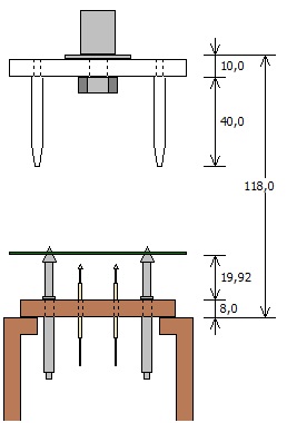 Z-axis visualizer
Macaos Gallery 1.4 (August 2016)
Macaos Gallery 1.4 (August 2016)
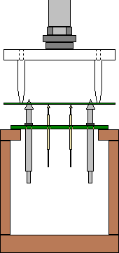
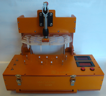
"Bed of Nails" test fixture creation
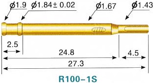
A "bed of nails" test jig is used for in-circuit testing of a PCB with components. Typically, the jig consists of a bottom fixture with many spring-loaded test pins (pogopins) that are placed to make contact with test points on the PCB. An upper fixture presses the board onto the bed of nails so that all of the pins make good contact. A test program may then be run to confirm the operation of the PCB. A test fixture is a plastic plate with holes drilled at each of the test point positions. Each test point hole will have a base (or receptacle) mounted in it. For each receptacle diameter, a spring-loaded pin head is inserted. You may choose from several different pin head styles, depending on the type of test point the pin will contact.
Test fixture creator moduleOpen a PCB product in the test fixture creator module and specify the parameters of the fixture plate. Then click on holes to place alignment pins, and click on holes or pads to place test pins. Once all pins have been placed, adjust the position of the press point and then center the PCB under the press point. The published test fixture product includes a drill file for the fixture plate and wiring list documentation. Top side fixtureIdeally, all of the test points should be on the bottom side of the PCB. However, if necessary, a top side fixture may also be created. If a test fixture already exists for a PCB, then you may choose to use that fixture to specify the placement of the PCB in the new fixture. Test accessoriesTest jigs, test pins and related accessories available for purchase from buy.macaos.com. |
Viewer improvementsLock cursor to axisPress Alt+X or Alt-Y to lock the cursor position to the current X or Y coordinate. Press Esc to release the lock. |
Macaos Gallery 1.3 (April 2016)
Macaos Gallery 1.3 (April 2016)
Product Browser Improvements
New product specifications and statistics
Numerous product parameters have been added to the Macaos system. This will improve online pricing and quality control. See the Import Module section (below) for a complete list.
Import module improvements
New product specifications:
- board type: rigid, flex, rigid-flex, metal-based-board
- depth routing
- flex stiffener (flex, rigid-flex only)
- cover layer (flex, rigid-flex only)
- thermal conductivity (metal-based-board only)
- via fill type
- flexible layers (rigid-flex only)
- carbon print
- kapton tape
- countersink
- half-moon holes
- microvias
- plated slots
- beveled edge (with angle and backoff)
New product statistics:
- holes/dm2
- minimum non-plated hole/edge to copper clearance
- qty routs
- minimum rout tool diameter
- total rout length
- estimated weight
- number of test points (solder mask openings)
Product options
- Performance class 2, 2+ or 3
- Impedance control to be done by manufacturer
- Do not allow manufacturer marking on board
- Do not allow copper shaving from board edges
New viewer functions
- d Highlight minimum width lines on each visible copper layer
- a Highlight minimum annular ring pads on each visible copper layer
- o Toggle show only centerline/outline of objects
Custom stackup definition
- It is now possible to indicate if a dielectric layer is core or prepreg in a custom stackup.
- It is now possible to indicate that a dielectric layer is flexible
- It is now possible to indicate that the thickness of a dielectric layer is impedance critical
Alignment of pick and place files
When aligning pick and place files, only the visible layer(s) will be moved. In this way, it is possible to make separate adjustments for top and bottom sides.
Panelization improvements
Place text
Allow text on notation layers to be placed within boards in a panel
Graphical remarks
Add graphical remarks to a panel.
Stencil improvements
Show potential errors
The stencil creator checks for stencil openings that do not appear to be consistent with the original stencil data. This could be due to the original openings having been reduced by the board designer, or because the stencil creator was not able to locate the correct reference pad on the copper layer. If potential errors are found, they can be highlighted for inspection.
Automatic fiducial detection
If the stencil data contains objects that appear to be fiducials, these are automatically detected and can be easily marked as fiducial or deleted. The same is true for stencil fiducials in a panel frame defined in the panel module.
Edit/split rotated shapes
The pad shape editor now works on shapes with any rotation factor.
Transfer objects from any layer
It is possible to copy objects from any layer to a stencil layer.
Assembly Data Manager
The Quick Help button opens a web page with step-by-step guidelines for generating an RFQ for Assembly.
Bill of Materials (BOM)
Before processing, a hint window reminds the user to specify column headers.
After processing, the rows of the output BOM are green if a single match is found, or yellow if multiple product matches are found.
Pro version improvements
Order packaging option
A new order option has been added to the Quotation module: Package in accordance with IPC-1601 (antistatic, humidity sensor, dessicant, etc)
Quotation quantities
When making price quotes for panels, the order quantity is always the number of panels. But it is now possible to specify number of boards, which will automatically be converted to number of panels in the price grid
Macaos Gallery 1.2 (September 2014)
Macaos Gallery 1.2 (September 2014)
Assembly Data Manager
The new Assembly Data Manager Module allows you to work with component purchasing and placement data for a PCB. You may also create and modify graphical remarks for a product.
Pick and Place Data (PnP)
PnP data specifies the designator, location and rotation of components that will be automatically placed for (usually) reflow solderinig. There are, unfortunately, a multitude of different PnP data formats. Macaos Enterprise is able to read more than a dozen of these formats. (See the user manual for details about the most common formats supported.)
With the Assembly Data Manager, you can do the following:
- View PnP data for top and/or bottom side
- Show/hide individual components. Hidden components are deleted from PnP data once the data is saved.
- Double-click on a component in the list to zoom into that component in the viewer.
- Import PnP data
- Align PnP data. If the PnP data does not have the same coordinate origin as the Gerber data, this can be corrected.
- Create PnP data. You can select one or more pads and define a PnP component or fiducial mark to be located at the center of the rectangle surrounding the selected pads.
- Edit PnP data. You can edit the designator, side, rotation and description text for any component.
Bill of Materials (BOM)
A BOM is a list of the components that are to be used with the printed circuit board. The BOM is used to select and purchase the correct components as well as to specify where each component should be placed on the printed circuit board.
In many cases, a BOM contains component descriptions that require some interpretation by the purchaser, due to inconsistent or incomplete specifications. The Assembly Data Manager attempts to improve the usability of the BOM by applying a number of parameter recognition techniques.
The procedure is as follows:
- Import a BOM. BOM data may be imported as a text file, an Excel .xls file, or copied and pasted directly from a spreadsheet program.
- Right-click on a row to mark it as the column headers or the first row of valid component data.
- Right-click on a column header to specify the type of information contained in the column
- Click on the Process (gears) button to process the list of components.
- A new spreadsheet is created with the interpreted parameters. If necessary, make corrections and click on the Retry button to do a new search.
- Once you are satisfied with the BOM, save the processed list to the product.
- The processed list may be exported to an Excel file.
Graphical remarks
Graphical remarks may be added to any product. Existing graphical remarks may be deleted or replaced, if desired.
A remark may be created as follows:
- Click on the Add remarks to board (yellow note) button.
- Draw a circle around the feature(s) to which the remark applies.
- Enter the remark text in the dialog box.
- Click OK.
To delete a remark, click on the Delete button and draw a selection rectangle around the entire remark.
If you need to change the text of a remark, you can click on the Edit button and change a single line of text at a time. Note: This can only be done with remarks created during the current session. For older remarks, you must delete and re-create the remark.
Stencil improvements
Split/replace openings
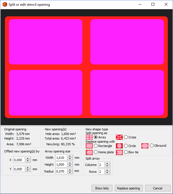
The module for splitting a large stencil opening into an array of smaller openings has been improved. It is now possible to choose between several split patterns or replacement opening shapes. You have full control over the size and shape of the new opening(s), as well as statistics to indicate how the change will affect total solder delivery.
Although this feature is primarily intended for working with large (heat sink) openings, it may be used to modify the shape of any opening in the stencil.
Highlight large pads
This feature allows you to easily locate stencil openings whose height and width are larger than the size you specify. This way you can quickly find opening that should be split.
Place board data relative to frame edge or frame center
It is now possible to specify the position of the board relative to the edge of the stencil frame, or relative to the center of the frame. Top and bottom side data may be offset horizontally or vertically, as desired.
Mirror bottom side data
Bottom side data is automatically mirrored, so that the squeegee side of the stencil will always be the top side of the stencil.
Import module improvements
Support for up to 30 copper layers
Macaos Enterprise now supports boards with up to 30 copper layers. This is an increase from the previous limit of 22 copper layers.
Full support for the latest Extended Gerber format (Gerber X2 rev J3)
A new version of the Extended Gerber file format was released in the spring of 2014. This version adds a structure for identifying the file format version, board layer or function of the file, and classes of features within the file. Macaos Enterprise fully supports reading and interpreting these extensions.
Support for Pick and Place files generated by Cadstar
Pick and place files generated by Cadstar may now be imported, either in the Import Module or in the Assembly Data Manager.
Panelization improvements
Place tabs in line
When placing break-off tabs on a panel, if you click and drag the mouse then a horizontal or vertical line is shown. When you release the mouse, a break-off tab will be placed at each point where the line crosses a board edge.
Panel drawing improvements
A table in the upper left corner of the panel drawing specifies the size of fiducials and bad marks. For a single-product panel, this table also specifies the X and Y step distance of the boards in the panel.
Product Browser improvements
Specify filenames when exporting to Gerber
When exporting a product to Gerber files for manufacture, you may choose one of two Macaos filename templates, or define your own template.
Macaos Gallery 1.1 (December 2013)
Macaos Gallery 1.1 (December 2013)
Import module improvements
Place a text string on the PCB
A text string may be placed on a notation layer of the PCB as follows:
- After linking files and creating an outer contour, click on the Add symbols to board (paintbrush) button, and then click on the Text button.
- Enter the desired text string.
- Select the text height, layer and text rotation, as desired.
- Move the mouse cursor to the desired position and click to place the text.
Add IPC/JEDEC J-STD-609A compliant marking to the PCB

The IPC/JEDEC J-STD-609A stanard defines how PCBs should be marked to identify the the presence (or absence) of lead and/or other attributes in a PCB or PCB assembly. The import module includes a simple dialog box where you can create a compliant text string and add it to a PCB by answering up to 6 questions about the laminate material, surface finish and (optionally) the required assembly processes. Once the text string has been generated, it may be placed at any location on the notation layer of the PCB.
While in Add text mode, click on the J-STD-609A button to open the dialog box. Select the appropriate parameters for the text string, and then click OK. Place the text string as described above.
Add remarks to the PCB graphically
You can add remarks to a PCB at a specific location. This is useful when a remark is tied to some feature or location of the PCB. A remark may be created as follows:
- After linking files and creating an outer contour, click on the Add remarks to board (yellow note) button.
- Draw a circle around the feature(s) to which the remark applies.
- Enter the remark text in the dialog box.
- Click OK.
Remarks are added to the Remarks layer. A circle will be drawn around the selected feature(s) and the remark text placed to the right of the circle.
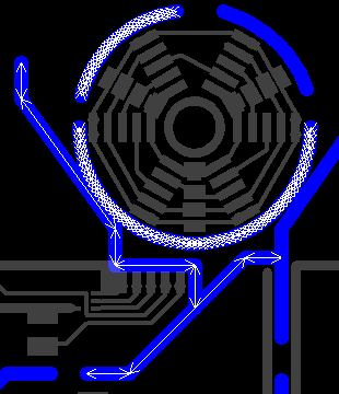
 Via protection (plugging, filling, etc)
All holes with a specific drill tool may be specified for via protection. To do this, right-click on the tool in the tool list (of the Drill tools tab) and choose the desired via protection type from the Via protection submenu. A new layer will be created indicating the via holes to be protected.
Create contour segments graphically
When defining an outer or inner contour, the contour must be defined as a closed polygon. If there are missing segments, these can by drawn. This may be done as follows:
- Click on the Draw contour segment (pencil) button.
- Move the cursor to the position where the segment will start. If desired, press the X key to snap the cursor to the nearest existing segment endpoint.
- Click to start the drawn segment.
- Move the cursor to the position where the segment will end. If desired, press the X key to snap the cursor to the nearest existing segment endpoint.
- Click to create the segment.
View endpoints of highlighted segments when creating contour
When selecting segments for a contour, the Show endpoints of highlighted segments causes the highlighted segments to be drawn with thin lines and arrowheads. This is useful when trying to see where a gap or overlap exists that prevents the selected segments from being recognized as a closed polygon.
Minimum features
Minimum track width and minimum annular ring are estimated by performing a simple analysis of the imported copper and drill layer data. Minimum clearance is estimated to be the same as the minimum track width. These estimates will be correct in most cases, but some CAD systems generate their trace and/or pad data in a manner that is too complex and time-consuming for the rapid analysis performed by the Import module.
If you know that one or more of the estimated values are incorrect, you should enter the correct values as necessary.
Import of ODB++ jobs
The import module now includes limited support for importing PCB jobs in ODB++ format. An ODB++ job may be imported as a .zip, .gzip, .tgz or .tar archive. When opening an ODB++ project, the layers, outer contour and drill tools are automatically imported and linked. The layers in from the ODB++ project are listed in the ODB++ Layers tab.
If a layer has been linked incorrectly, right-click to link it to a different layer. If the board has inner contours, track routing or scoring, then these must be specified in the normal manner. The stackup, finish and mask colors must also be specified.
If the ODB++ project contains multiple steps, you must choose which step to open. In most cases, one step will be the board and another step will be a panel containing the board. If you are unsure which step to open, choose any step. After viewing the step, you can reopen the file to view a different step, if necessary. The import module has some limitations when working with panelized steps, so we recommend importing the board step and using the Panelization module to create your panel.
Note: Import of ODB++ files is a new technology in the Import module. It has not yet been widely tested by Macaos. Please inspect your board carefully before publishing. If you encounter problems, you can help us improve the ODB++ engine by using the Help|Send problem report command to send us your files together with a description of the problem.
Import of HPGL files
The Import Module has limited support for plotter files in HP-GL format. HP-GL files may be included in a product for documentation purposes only.
Due to the nature of the HP-GL format it is not possible to reliably detect an HP-GL file without parsing the entire file. Therefore, the Import Module detects HP-GL files as Text (or Other, if the file contains plotter setup escape sequences).
To view an HP-GL file, right-click on the file name and choose Change file type|HP-GL. The file will be displayed in the viewer. To include the file in a product, link the file to a User layer. It is not possible to link an HP-GL file to any other layer.
Align pick and place files with Gerber data
If the coordinate origin of pick and place data is different from that of the Gerber data, the offset can be aligned in the same manner as when aligning drill data with Gerber data.
Panelization improvements
Flip board in panel
An individual board in a panel may be flipped upside-down. When a board is flipped, it is mirrored and all of its layers are swapped from top to bottom (and vice versa). This is useful when creating a panel where it is desirable to use the same solder paste stencil for both sides of the panel, or when necessary to improve the copper balance of the panel.
To flip a board, press Shift+Space while the mouse cursor is above the board to be flipped. (The board does not need to be selected.
Clear zone for fiducials
The clear zone around a fiducial mark may be specified as the diameter or width of a circle or square (depending on the soldermask shape). When copper fill is selected for outer layers, then the copper fill will be removed from the clear zone of each fiducial.
Pull scoring line back from panel edges
Scoring lines extend normally from one edge of a panel to the opposite edge. Individual scoring lines may be pulled back from the outside panel edge to the inside edge of the panel frame by holding the mouse cursor over the end of the scoring line and pressing Ctrl+V. Note: Manufacturing a panel with this feature requires Jump Scoring. Not all manufacturers are able to deliver panels with Jump Scoring.
Copper fill on inner layers
Copper fill on inner layers is now generated as a pattern of 5mm diameter dots rather than as solid copper..
Product number layer for multi-product panels
When working with multi-product panels, an additional Product number layer shows the placement and product number of each board in the panel. This layer is for documentation purposes only and may not be exported as a manufacturing layer.
Stencil improvements
Define reduced thickness region based on objects from any layer
When defining a reduced thickness region based on selected objects, the objects may be selected from any layer. The reduced thickness region may either be a rectangle surrounding the selected objects, or may follow the shape(s) of the selected objects plus an "oversize" dimension.
Viewer improvements
View from below
Press the M key to toggle the view between view from above and view from below. When viewed from below, the board is mirrored and only the bottom side layers are visible. This is useful if you wish to see what the bottom side of the product will look like.
Rotate view
Press the R key to toggle the view between unrotated and rotated by 90 degrees. This is useful when viewing a tall, narrow board to make it fit better into the available screen space.
Screen dump
Press Ctrl+V to copy the product viewer image to the clipboard. Press Ctrl+Shift+V to save the product viewer image as a file in PNG (Portable Network Graphics) format.