Assembly Data Manager (ADM)
Assembly Data Manager (ADM) BruceThe Assembly Data Manager (ADM) is an integrated BOM Tool and Pick and Place Data Manager for PCBs. It provides an environment for managing and reviewing Pick and Place (PnP) and Bill of Materials (BOM) data.
An integrated, standards-based solution
The ADM helps dramatically reduce time and effort in preparing assembly data, by combining the following features in a single module:
- Graphic viewer with component editing functionality
- Structured component overview with properties editor
- Component search facility
- Send RFQ for assembly to participating EMS providers (Enterprise Basic version only)
- Component rotation, height and solder temperature editor
- Component price estimator (EMS version only)
- Export PnP and BOM data (EMS version only)
The ADM makes use of the Gerber Format X3 extensions1 to combine PnP, BOM and Assembly Drawing data into an integrated component layer of a PCB product. As CAD systems2 implement these extensions, a rapid and error-resistant path from designer to manufacturer may be achieved.
The component layer displays the location, rotation, size and key pin location of each component together with properties such as manufacturer part number, supplier SKUs, height, max solder temperature, etc. The use of a standards-based structure for this information allows purchasers, supplers, process line operators, etc to automate their systems and thereby reduce costs.
Including test points in your imported PnP data (or defining them in the ADM) makes them available to the Test Fixture Designer. Components with a TPxx designator are automatically assigned to the Test Point component class and marked as Do Not Place during import. The Test Fixture Designer will import each Test Point component and create a corresponding test pin. Note: For best results, all test points should be on the same side of the PCB.
1 Macaos actively participates in the development of these standards.
2 Some CAD systems, such as kicad, already support Gerber X3 output.
An efficient and straightforward workflow
- Import PnP data. (This may already have been done when the PCB product was imported.) This should be done prior to importing BOM data.
- If necessary, align the PnP data with the PCB data.
- Import BOM data. (This may already have been done when the PCB product was imported.)
- If necessary, move new components to their correct position. BOM components are matched to PnP components by their designators. BOM components which are not found in the PnP data are placed to the left of the PCB. Each of these should be moved to its correct position on the PCB.
-
If available, import test pad data in IPC-D-356 format. (This may already have been done when the PCB product was imported.) If necessary, align the test pad data with the PCB.
-
If test pad data exists, run the Merge action to extract key pins and footprint outlines from the test pad data.
- Draw outlines and mark Key Pins. For assembly purposes, it is desirable to graphically display the size and orientation of each component. This information is typically not included in the imported PnP or BOM data, but it can easily be added by drawing outlines and marking key (1 or A1) pins.
- Check/edit the properties of each component. Ideally, a complete manufacturer part number should be specified for each component. At the minimum, each component description should be unambiguous. The edit module includes an online component search function (powered by Octopart) to aid in quickly specifying unambiguous manufacturer part numbers.
- Save changes to the product and generate reports as desired.
Component List
The component list has three levels. At each level, two icons show whether or not the BOM and Placement status of the components has been checked and approved.
- The component class (resistor, capacitor, connector, etc).
The green icon indicates that the BOM status has been approved for all components in the class.
The blue icon indicates that the Placement status has been approved for all instances in the class. - The component (a single part number). When editing a component, you can change the properties which apply to all instances of that component.
The green icon indicates that the BOM status has of the component been approved.
The blue icon indicates that the Placement status has been approved for all component instances. - The component instance (at a specific location). When editing a component instance, you can change the rotation and placement status of that instance.
The blue icon indicates that the Placement status has been approved for the component instance.
The other icon which indicates whether the component is a fiducial mark, should not be installed, is a PnP component or is a non-PnP component. The icon also indicates whether the component is on the top or bottom layer.
Clicking on a component or instance displays its properties in the component editor. Double-clicking also zooms the viewer to the component. Right-click on the component list to specify the zoom size. You can also press Ctrl+Z to zoom to the selected component/instance, Ctrl+E to edit the selected component/instance or Ctrl+D to edit and open the online search module.
Note: If two or more component instances are grouped together, even though they should not be, this can be corrected by changing the Manufacturer Part Number of the instance(s) to be removed from the group. To do so, select the instances to be modified, right-click and select Change part number of instance and then enter the correct part number.
Clicking on the Highlight instance button zooms the viewer to the selected component and highlights it with three concentric circles. Clicking on the Highlight all instances button zooms the viewer to all instances (on the same side) as the selected component and highlights each of them with three concentric circles. If Highlight instance pads is checked, then all of the component’s pads will also be highlighted. Note: Highlighting pads is not supported unless IPC-D-356 data has been imported.
To search for a component in the list, type the designator in the text box at the bottom of the component list. It is also possible to enter a range of designators, such as C13-C25. The tree buttons may be used to expand or collapse the component list. The Exclude from list buttons may be used to hide components which are approved or have a specific placement status.
Component Alerts
A component alert indicates that the component needs further attention. When importing PnP or BOM data, setting the check mark for a component creates a component alert. These components have red text in the first column of the component list. Right-click on a component instance (or press Alt+A) to toggle the alert status of the selected components. Note: Component alerts are not saved with the product. You should resolve all alerts before closing the ADM.
Component display
Graphically, how a component displays depends on how much information about the component has been specified. At the minimum, a 0.3 mm circle is drawn at the component’s location (centroid/pick point).
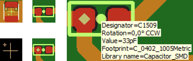
- If only the component’s location and rotation are specified (typically if imported from PnP data), then the component is displayed as a 20-pixel cross with a 5-pixel cross toward the unrotated component’s upper left corner. In other words, if the component rotation is 90 degrees, then the 5-pixel cross will be in the lower left corner. The cross symbols are always 20 and 5 pixels, regardless of zoom factor. Note: The 0.3 mm circle is not drawn when the zoom factor is so high that it would hide the 5-pixel cross.
- Components where the location is not specified (typically if imported from BOM data) are placed to the left of the PCB, with 10 mm spacing.
- If the component outline has been specified, then the outline is drawn with a 0.1 mm line. In this case, no 20-pixel cross is shown.
- If the location of the key pin (typically pin 1 or A1) is specified, then a 0.36 mm diamond is drawn at the location of the key pin. In this case, no 5-pixel cross is shown.
Press the Ctrl key and hold down the left mouse button on a component to view component properties such as designator, rotation, value, manufacturer part number, etc.
Press the Ctrl and Alt keys and click a component to locate it in the Component list.
Component rotation
A component’s rotation specifies how the component is rotated from it’s nominal position when placed on the PCB. IPC-7351 specifies the nominal, or 0°, rotation as follows:
- For two-lead components, the key pin is (pin 1, + or cathode) is at the left
- For components where the key pin (1 or A1) is near a corner, that corner is at the upper left
- For components where the key pin is at the center of a side, the key pin is at top center
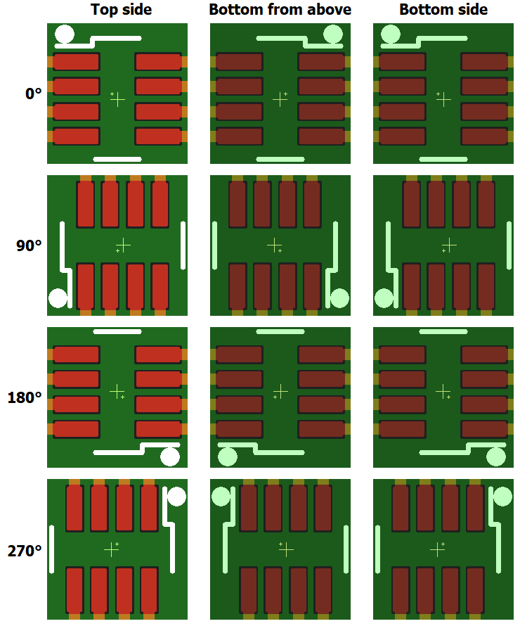
If the component is placed on the bottom side of the PCB, then the above rules apply as if viewed from the bottom side. This means that when viewed from the top side, the component is mirrored along the X-axis (left/right swapped).
Rotations are always specified as counter-clockwise. However, due to the mirroring, when viewed from the top side, components on the bottom will appear to be rotated clockwise.
The image to the right shows how bottom side components will appear when viewed from the top side (middle column) and when viewed from the bottom side (right column).
Graphic operations
A number of graphic operations are available:
Importing PnP data
Importing PnP data BrucePnP data is usually generated by the CAD system used to design the PCB. If PnP data is not available, it can be created manually.
Typically, PnP data consists of four, five or six values per component:
- Designator
- X position (typically in mm, inch or mil)
- Y position (same unit of measure)
- Rotation in degrees (usually counter-clockwise)
- Description (perhaps in several columns)
- Side (top or bottom; bottom sometimes called mirrored)
Click on the Import button in the Pick and place actions toolbar to select a PnP file for import. Alternatively, click on the small down-arrow in the lower right corner of the button to import a file which is already attached to the product.
Some CAD systems generate separate top and bottom PnP files. In this case, use the Bottom button to import the bottom side PnP file.
Macaos automatically imports several PnP formats. For those which are not recognized, or which have some level of ambiguity, the Pick and Place Data Import dialog box helps to specify how the data should be interpreted for import.
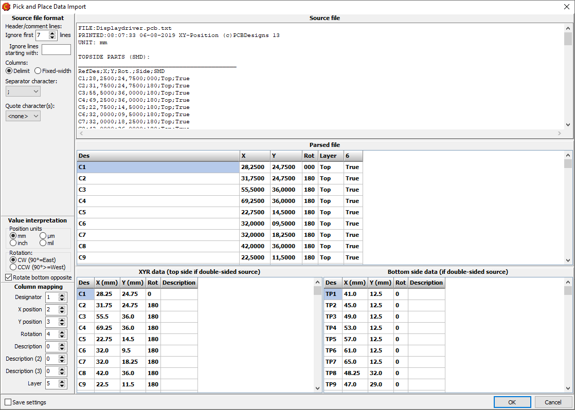
- If necessary, the source content may be edited, either directly in the text of the source file, or in individual cells of the parsed file.
- If necessary, specify the number of header rows to ignore, and the prefix character for comment lines.
- Specify whether the input file has delimited or fixed-width columns. For delimited columns, specify the delimiter character (and quotation character, if necessary). For fixed-width columns, specify the column widths.
- Specify the unit of measure used for X and Y coordinates. If incorrectly specified, the scale of the component layer will not match the scale of the PCB.
- Specify whether rotations are clockwise or counter-clockwise. Normally, bottom side component rotations should be imported in the opposite direction. If this doesn’t work with your file format, remove the check mark from Rotate bottom opposite.
- Normally, bottom side rotations are flipped horizontally (around the Y-axis). For PnP files which flip the rotation vertically (around the X-axis), such as those from Altium, set a check mark at Flip bottom vertically.
- Specify the input column numbers for each output field.
If there are components that might need further attention after import, set a check mark by each of them. This will create a component alert, and the component will be highlighted with red text in the component list. Note: Component alerts are not saved with the product. You should resolve all alerts before closing the ADM.
Once the data format has been correctly specified, click the OK button to import the data.
If necessary, align the component layer with the PCB.
Fiducial marks
Most Pick and Place systems expect there to be three fiducial marks on the board, typically near each of three corners. The locations of these fiducial marks need to be included in the PnP data.
If the board does not have dedicated fiducial marks, other optically distinct features, such as through-hole pads, may be used. Note: Via holes covered with solder mask are usually not suitable as fiducial marks.
- Left-click and draw a rectangle around the pad to use as a fiducial mark.
- The fiducial mark is added at the center of the selected pad.
Note: If a pad (from the originally imported Gerber data) is drawn (as one or more wide lines/arcs) rather than flashed (as a single shape object) then it will not be identified as a pad in the above procedure. In cases where no pads are found within the selection rectangle, the (center of the) selection rectangle is used.
Creating PnP data manually
If PnP data is not available for a component, it may be created manually, as follows:
- If a similar component already exists, select it in the component list to copy its properties to the new component.
- Left-click and draw a rectangle around all pads of the component to create.
- Specify the component designator and (if desired) specify that component properties should be copied from the selected component. The new component designator must be unique.
- The component is added at the center of the selected pads.
Tip: Import BOM data prior to creating components manually. Components found in the BOM data which do not exist in the PnP data are automatically created and placed to the left of the PCB. They may then be moved to their correct position.
Note: If a component pad (from the originally imported Gerber data) is drawn (as one or more wide lines/arcs) rather than flashed (as a single shape object) then it will not be identified as a pad in the above procedure. In cases where no pads are found within the selection rectangle, the (center of the) selection rectangle is used.
Align component layer with PCB
Align component layer with PCB BruceUsually, the coordinates in an imported PnP file will have the same origin as the PCB. If not, then the component layer must be aligned with the PCB data, as follows:
- Left-click and draw a rectangle around a component in the component layer. Once selected, a rubber-band stretches from the component to the mouse pointer.
- Left-click and draw a rectangle around all of that component's pads on the PCB.
- The selected component is moved to the center of the selected pads, and all other components are moved the same distance.
Tip: It is often easiest to choose a relatively large hole-mounted component that does not have any vias near the boundaries of the rectangle that encloses the component's pads.
Note: If a component pad (from the originally imported Gerber data) is drawn (as one or more wide lines/arcs) rather than flashed (as a single shape object) then it will not be identified as a pad in the above procedure. In cases where no pads are found within the selection rectangle, the (center of the) selection rectangle is used.
Importing BOM data
Importing BOM data BruceBOM data is typically a list of components and their properties. It's main purpose is to specify the components for purchasing. Macaos can import BOM data from a text file or from an Excel .xls spreadsheet file. In both cases, the data must be in a table form, where each row represents a component and each column represents a single component property (such as designator, manufacturer part number, value, etc).
Click on the Import button in the Bill of materials actions toolbar to select a BOM file for import. Alternatively, click on the small down-arrow in the lower right corner of the button to import a file which is already attached to the product.
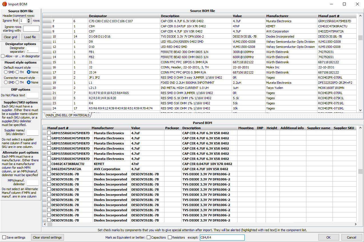
A spreadsheet file is loaded directly into the Import BOM dialog box. When importing a text file, the format must first be specified (much like when importing PnP data). It is also possible to copy data from an open spreadsheet directly into the Source BOM file grid (by right-clicking the cell that will become the top left corner of the pasted data).
 To import the BOM, do the following:
- If necessary, specify the number of header rows to ignore, and the prefix character for comment lines to ignore.
- Where possible, the column contents are automatically identified. (This may not always be accurate, so automatic column mappings should be checked.)
- Specify the input column mapping for the remaining output fields by clicking on source column headers and selecting the column contents. For the Value, Package, Description, and Additional info output columns, multiple input columns may be mapped. This is also true for the Supplier/SKU fields and the Alternate MPN/Manufacturer fields.
- Specify parameters for individual columns, as necessary.
Designator: If the designator field lists multiple designators, specify the separator character (typically a comma, semicolon or space). The import module automatically converts designator ranges like C2-4 or C2..4 to individual designators (C2, C3 and C4). Set a check mark on Allow – or .. in designator to prevent designator range conversion.
Value: Any number of source columns may be mapped to the Value column. The contents of the source columns will be concatenated, separated by a space character.
Description: Any number of source columns may be mapped to the Description column. The contents of the source columns will be concatenated, separated by a space character.
Mounting style: If a column is mapped, you must specify an SMD text and a Thru-hole text. Components which match one of these texts will be assigned a mounting style of SMD or TH (respectively). The mounting style will remain unassigned for components which do not match.
If no column is mapped, you may select a default mounting style, which will be applied to all components (except connectors). A separate default style may be specified for connectors.
Do not place: Specify a Do not place text. Components which match this text will be marked as not to be installed.
Additional info: Any number of source columns may be mapped to the Additional info column. The contents of the source columns will be concatenated to the component’s Original description property, separated by a space character. (The Original description property is the normally the component description imported from Pick and Place data.)
Supplier name and SKU: Supplier names and SKUs must be paired. They can be taken from a single source column or from pairs of source columns. If there are multiple values in a column, then a delimiter text must be specified. Typical delimiters are comma, semicolon or space.
- If the supplier name and SKU are in a single column, specify the source column as the Supplier SKU column and specify the character that separates the names and SKUs. (The supplier name column must not be mapped.)
For a single pair, the column content must be Name<delimiter>SKU.
For multiple pairs: Name<delimiter>SKU<delimiter>Name<delimiter>SKU... - If the source has separate columns for supplier name and SKU, specify both source columns. If each column has multiple values, then specify the character that separates the values. It is also possible to map multiple pairs of columns.
Alternate part numbers: Manufacturer names and MPNs must be paired. They can be taken from a single source column or from pairs of source columns. If there are multiple values in a column, then a delimiter text must be specified. Typical delimiters are comma, semicolon or space.
- If the alternate manufacturer name and part number are in a single column, specify the source column as the Alternate MPN column and specify the character that separates the names and SKUs. (The Alternate manufacturer column must not be mapped.)
For a single pair, the column content must be Name<delimiter>MPN.
For multiple pairs: Name<delimiter>MPN<delimiter>Name<delimiter>MPN... - If the source has separate columns for manufacturer name and MPN, specify both source columns. If each column has multiple values, then specify the character that separates the values. It is also possible to map multiple pairs of columns.
It is possible to edit the text in either grid, by clicking on a cell and entering the desired text. You can change the text in an entire column, or in selected cells, by right-clicking on the grid. It is also possible to add an extra column to the source grid (for example, to add mounting style data). Note: In most cases, it is best to edit the source grid, since changes to the parsed grid will be lost if any of the column mapping parameters are changed.
Check off for Save settings to store column mapping parameters as default values for future BOM import. Click on the Clear stored settings button to reset all column mapping parameters and default values.
If there are components that might need further attention after import, set a check mark by each of them. This will create a component alert, and the component will be highlighted with red text in the component list. Note: Component alerts are not saved with the product. You should resolve all alerts before closing the ADM.
Components may be automatically marked as allowing equivalent or better alternates to the specified manufacturer part number if any of the Mark as Equivalent or better boxes are checked. By default, all components of the specified type(s) will be marked. To exclude components from being so marked, their designators should be listed in the except list, separated by commas (without spaces).
Once the data format has been correctly specified, click the OK button to import the data.
Components in the BOM which do not already exist on a component layer are automatically placed in a 10 mm grid to the left of the PCB. These should be moved to their correct location.
Move components
Move components BruceWhen a component is imported without a location, it is automatically placed to the left of the PCB on a 10 mm grid. These components should be moved to their correct location, as follows:
- Left-click and draw a rectangle around the component to move. Once selected, a rubber-band stretches from the component to the mouse pointer.
- Left-click and draw a rectangle around all of that component's pads on the PCB.
- The component is moved to the center of the selected pads.
Note: If a component pad (from the originally imported Gerber data) is drawn (as one or more wide lines/arcs) rather than flashed (as a single shape object) then it will not be identified as a pad in the above procedure. In cases where no pads are found within the selection rectangle, the (center of the) selection rectangle is used.
Outlines and Key Pins
Outlines and Key Pins BruceThe component outline and location of the key pin are important visual cues for the operators who mount components on a PCB. This is especially true for polarized components with a symmetrical footprint.
Outlines
Component outlines typically follow one of four patterns:
- Body tightly encloses the component body
- Lead-to-lead encloses the component body and all component leads
- Footprint tightly encloses all of the component pads
- Courtyard encloses the footprint and the component body
By default, Footprint outlines are created, though this may be overridden by pressing the Ctrl key to create a Body outline. The procedure is:
- Double-click on a component in the component list to select it and make it visible in the viewer.
- Left-click and draw a rectangle around all of the component pads. A Footprint outline (which tightly encloses the selected pads) is created.
- If you press Ctrl when drawing, then instead the drawn rectangle becomes the Body outline.
- The outline will be applied to all instances of the selected component.
Note: If a component pad (from the originally imported Gerber data) is drawn (as one or more wide lines/arcs) rather than flashed (as a single shape object) then it will not be identified as a pad in the above procedure. In cases where no pads are found within the selection rectangle, the selection rectangle is used to define a Body outline.
Right-click on a component or component instance to delete it's outline. If an instance is chosen, then only that instance's outline will be deleted. If a component is chosen then the outline will be deleted from all instances of that component.
Key pins
The key pin of a component is pin 1, pin A1, Cathode or Plus. Marking the location of the key pin gives operators a reliable visual reference to the component rotation. This is especially important for PnP components, to help insure that the specified rotation is correct when programming the automatic placement machine.
IPC-7351 specifies the most commonly used definition of component orientation. For an unrotated component, when viewed from above, the key pin is at the left (for 2-pin components). For multi-pin components it is near the upper left corner (or upper center) of the component outline.
To mark the key pin of a component, do the following:
- Double-click on a component in the component list to select it and make it visible in the viewer.
- Left-click and draw a rectangle around the pad for pin 1 (or A1 or Cathode or Plus).
- The key pin will be marked for all instances of the selected component.
Note: If a component pad (from the originally imported Gerber data) is drawn (as one or more wide lines/arcs) rather than flashed (as a single shape object) then it will not be identified as a pad in the above procedure. In cases where no pads are found within the selection rectangle, the (center of the) selection rectangle is used.
Right-click on a component or component instance to delete it's key pin. If an instance is chosen, then only that instance's key pin will be deleted. If a component is chosen then the key pin will be deleted from all instances of that component.
Test pad (IPC-D-356) data
Test pad (IPC-D-356) data BruceWhen opening an IPC-D-356 file, the test pads for both the top and bottom sides are extracted to the Test pads top and Test pads bottom layers, respectively. The net name, designator and pin number is also extracted for each test pad. Other information in the IPC-D-356 file is ignored.
Most CAD systems can generate an IPC-D-356 file, which contains important information for electrical test of the bare PCB during manufacture. Since only a subset of this information is imported to the test pads layers, the complete file is also attached to the product, so that it is available to the manufacturer.
Note: Do not confuse test pads with test points or test pins.
-
Test pads are the locations for bare-board testing of the PCB during manufacture, which are extracted from an IPC-D-356 file to the Test pads layers.
-
Test points are specific pads or pins on the PCBA which would be used for in-circuit testing. For each test point, a “component” (with the Test point component class) should be added to the appropriate component layer. Ideally, test points (with TPxx designators) should be included in Pick and Place data, but they may also be created manually.
-
Test pins are the pins in a test fixture which will make contact with the PCBA during in-circuit testing.
Merge action
For each component on a component layers, the corresponding test pad layer is scanned for test pads with a matching designator.
-
A Footprint outline is derived from the outlines of all pins.
-
If the component has more than two pins, then pin 1 or pin A1 is marked as the key pin. If there is no pin 1 or pin A1, then pin B1, A2 or B2 is marked (if found).
-
If the component has two pins, if one of the pins has a pin number beginning with K or C (for cathode) or P (for plus), it is marked as the key pin. Otherwise, no key pin is marked.
Edit components
Edit components BruceComponent properties are shown in the column between the component list and the graphic viewer. Which properties may be edited depends on which level in the component list is chosen. Component properties may be edited as follows:
- Select a component in the component list, right-click and choose Edit component (or press Ctrl+E). This puts the ADM module in edit mode. Alternatively, choose Search component (or press Ctrl+O) to enter edit mode and open the component search module in a single operation.
- Edit properties as necessary.
- After making necessary changes, click on the OK buttonor press Ctrl+S to update the component.
Note: There is nothing to edit when the component class level is chosen.
Editing a component instance
When editing a component instance, the Rotation, Include in PnP output and Do not place properties may be edited. Once these properties are confirmed to be correct, the instance should be marked as Approved for placement.
Component instances which have been approved for placement display a blue check mark in the component list. If all instances have been approved, a blue check mark is shown at the component level as well.
Each component instance also displays a placement icon, based on the component layer and the state of the Include in PnP output and Do not place properties. Note: The Mounting style property does not affect the placement icon.
Editing a component
When editing a component, the bill of materials and process parameter properties may be edited.A primary goal when preparing a BOM is that each component be unambiguously specified, preferably with a complete manufacturer part number. For components (such as resistors) where a specific manufacturer is not critical, then all necessary parameters should be specified so that there will be no doubt which component the purchaser should acquire.
For components (such as resistors) where a specific manufacturer is not critical, the component may be marked as Equivalent or better by use of the check box or by right-clicking on the Alternate parts list. For these components it is important that all necessary parameters be specified, so that there will be no doubt which component the purchaser should acquire.
Once these properties are confirmed to be correct, the instance should be marked as Approved for BOM. This adds a green check mark to the component list. If all components have been approved, a green check mark is shown at the component class level as well.
Component search
When editing a component, you may click on the Search button to open the component search module. This displays relevant component properties for searching. Put a check mark beside the properties to use in your search (modifying texts as necessary) and click on the Search button.
Note: Access to the Octopart component database (through the Nexar Legacy API) is sponsored by the sales office for Macaos Enterprise users who are active customers. Macaos Enterprise EMS users and other users must acquire an API token from Octopart. Tokens for a limited number of searches per month are available at no cost.
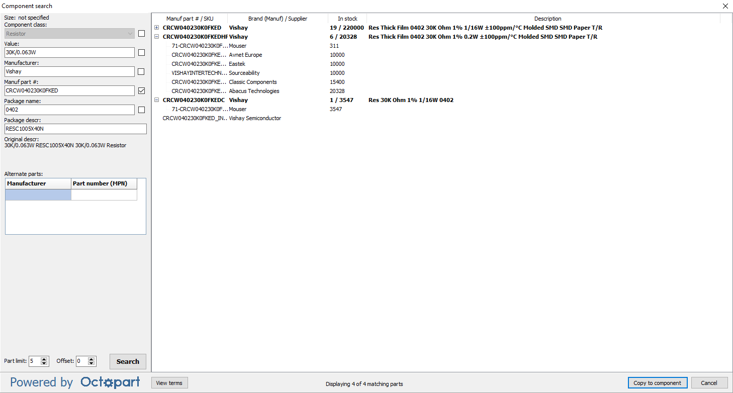
By default, up to 5 matching parts are returned in the list. This Part limit may be changed, if desired, up to a maximum of 20 per search. If more than 20 matching parts are found, the Offset may be used to specify how many parts to skip before returning a list of matching components.
For each stocked component, the quantity of suppliers and maximum inventory are listed. This gives a good estimate of the component’s availability.
With search results you can do the following:
- Set a check mark in the Manuf part # column to use the search result's Manufacturer and Manuf part # properties. The selected property values are shown at the bottom left, above the Search button.
- Set a check mark in the Alt column to add the search result to the Alternate parts list
- Right click on a search result to open the Octopart web page for the component
Once the desired Manuf part # (and alternates, if any) have been selected, click on the Copy to component button to update the component's properties in the component editor.
Additional editor operations
Some operations may be performed on multiple components. To do this, select one or more components (pressing the Ctrl and Shift buttons as necessary) and then right-click on the list.
- Edit Mounting style
- Edit Height
- Edit Max solder temp
- Change component class to...
For these four operations, the chosen property/properties of all instances of all selected components will be modified, regardless of whether selected at the component or the instance level.
- Mark status approved
- Mark BOM status approved or Remove BOM status approval
- Mark Placement status approved or Remove BOM status approval
- Remove approval
For these four operations, the Approved for placement property is marked or unmarked for all selected instances and the Approved for BOM property is marked or unmarked for all selected components.
- Mark as Do Not Place
- Remove Do Not Place
- Include in PnP output
- Exclude from PnP output
For these four operations, the Do not place or Include in Pick and Place output property is marked or unmarked for all selected instances. Selections at the component level of the list are ignored.
- Mark as Equivalent or better
- Remove Equivalent or better
- Remove all alternate part #s
For this operation, the text Equivalent or better is added to the list of alternate manufacturer part numbers for all instances of all selected components, regardless of whether selected at the component or the instance level.
- Swap layer
- Delete component
For these two operations, the operation is performed on all selected component instances. Selections at the component level of the list are ignored.
Note: When selecting multiple components with the Shift key, all instances between the selected components in the list will also be selected, even if the instance level is collapsed. However, if the last item selected is a component, then its instances will not be selected (since the parent is the last item in the selection range).
Request for Quotation
Request for Quotation BruceOnce your PnP and BOM data are ready, you can send a Request for Quotation (RFQ) for purchasing and assembly of your PCB to any participating Electronics Manufacturing Services (EMS) provider. This is a quick and easy way to get your PCB into production, since Macaos Enterprise makes the necessary information available to your partners in a reliable and orderly manner.
Note: This feature is only available for Macaos Enterprise users in markets with participating EMS providers.
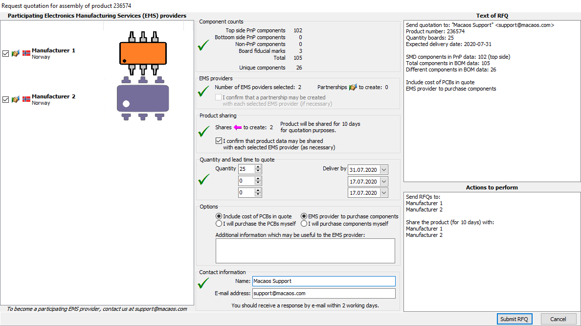
Generating an RFQ for assembly does 3 things:
-
If one does not already exist, a partnership is created between your company and each selected EMS provider.
-
The product must be shared with each selected EMS provider. If not already shared, then the product is shared with Quote visibility for 10 days.
-
A message is sent to each EMS provider informing them of your RFQ. The message is also visible in the EMS provider's Macaos Enterprise, together with your product data.
Icons in the EMS provider list indicate:
-
if you have already shared the product with the EMS provider
-
if the EMS provider is already your partner, but the product hasn't been shared with them
-
the country where the EMS provider is located
There are several bits of information that must be gathered before you can send an RFQ. Missing or inadequate information is flagged with a red X and an error message.
Once everything is ready, the message to the EMS providers is shown, as well as a list of actions (creating partnerships and shares, and sending RFQs) to perform. Click on the Submit RFQ button to perform these actions.
You may specify up to 3 different quantities and up to 3 different delivery dates for your quotations.
Normally, the EMS provider will purchase the boards and components for you. In the options section, you may choose to do some of your own purchasing.
Normally, EMS providers will respond by e-mail within two working days. If you choose to accept a quotation from one of the Macaos system EMS providers, you will need to contact them directly to place your order. You should also change the product share for that partner, giving them Manuf visibility and extending the lifetime of the share. See Product sharing for more information.
If a product is shared to an EMS provider with Quote visibility, then your partner will be able to view your PnP data and BOM list, but they will not be able to export that data from Macaos Enterprise.
Note: It is not possible to generate an RFQ for a product that a partner has shared with you.
Reports
Reports BruceBOM reports
Four different BOM reports may be viewed:
- Component list lists all components, grouped by component class
- Supplier list lists all components, grouped by supplier
- Placement list lists all component instances grouped by layer and mounting style
- Solder temperature report lists all components where the maximum solder temperature has been specified
Double-click on a component in the BOM report to edit the component.
Entering a search text causes all cells containing that text to be highlighted.
Note: Users with a Macaos Enterprise EMS license may export any of these reports to an Excel file.
Export of PnP data
Note: Access to this feature requires a Macaos Enterprise EMS license.
Pick and place data may be exported as a delimited text file. The column order, unit of measure, rotation direction, delimiter and layers may be specified to give the desired export format.
Price estimates
Note: Access to this feature requires a Macaos Enterprise EMS license.
When a manufacturer and part number have been assigned from a search result, an Octopart ID code is attached to the part number. This is indicated by a dollar sign together with the green Approved for BOM icon in the component lists. This ID code enables acquiring price estimates for the component.
You can right-click on a component class and choose Link to Octopart to automatically attach an Octopart ID code to components where the Octopart database has one (and only one) part with a manufacturer part number which exactly matches the component's part number.
Click on the Price button to open the Component pricing estimator module. This module lists all of the components that have an ID code and price offers (in various currencies) from available suppliers. In addition, all suppliers and all currencies are listed at the left.
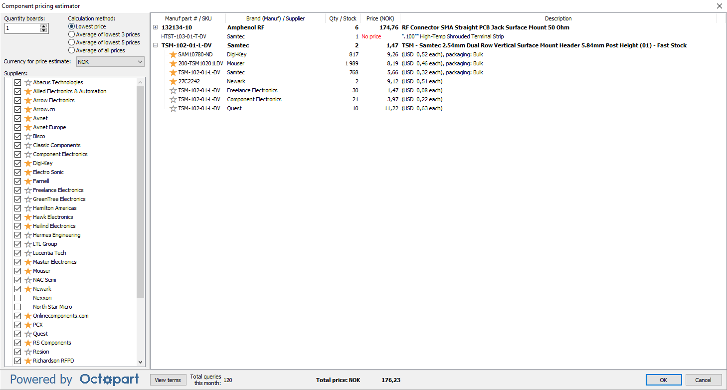
Specify the Quantity boards to be produced, select a Calculation method and the desired Currency for price estimate. If desired, remove the check mark from any suppliers to exclude when calculating the total price. The total price is automatically updated when a parameter is changed.
For each component, the manufacturer part number, manufacturer, quantity required (for the specified board quantity), estimated price and component description are listed. Right-click on a component to open the Octopart web page for the component.
Click on the small + (plus) button to the left of a manufacturer part number to see details of the supplier offers (with sufficient stock) for that component. For each supplier, the SKU, supplier name, quantity in stock, price in desired currency, price in supplier’s currency and packaging (if known) are listed.
Suppliers with a yellow star are authorized distributors for the manufacturer. Suppliers with a gray star outline are non-authorized stocking distributors. Suppliers without a star are brokers. See https://octopart.com/authorized for a description of these supplier classifications.
The price estimator converts all prices to the desired currency (using Octopart’s exchange rate) when calculating the total price. In the Description column for each offer, the actual price in the original currency is shown. The total price estimate for all components (with prices) is shown at the bottom of the price estimator module.
Note: All price offers are provided by suppliers through Octopart. Macaos Software AS bears no responsibility for the accuracy, fitness or usability of price offers presented in this module.
Clear all components
Clear all components BruceClick on the Clear button to delete all components from both sides of the board.
This operation is useful if you find that import of PnP and/or BOM data has not turned out well, and you wish to start over.
Note: This operation can not be undone. However, you can exit the module without saving changes in order to revert to the previously saved state.