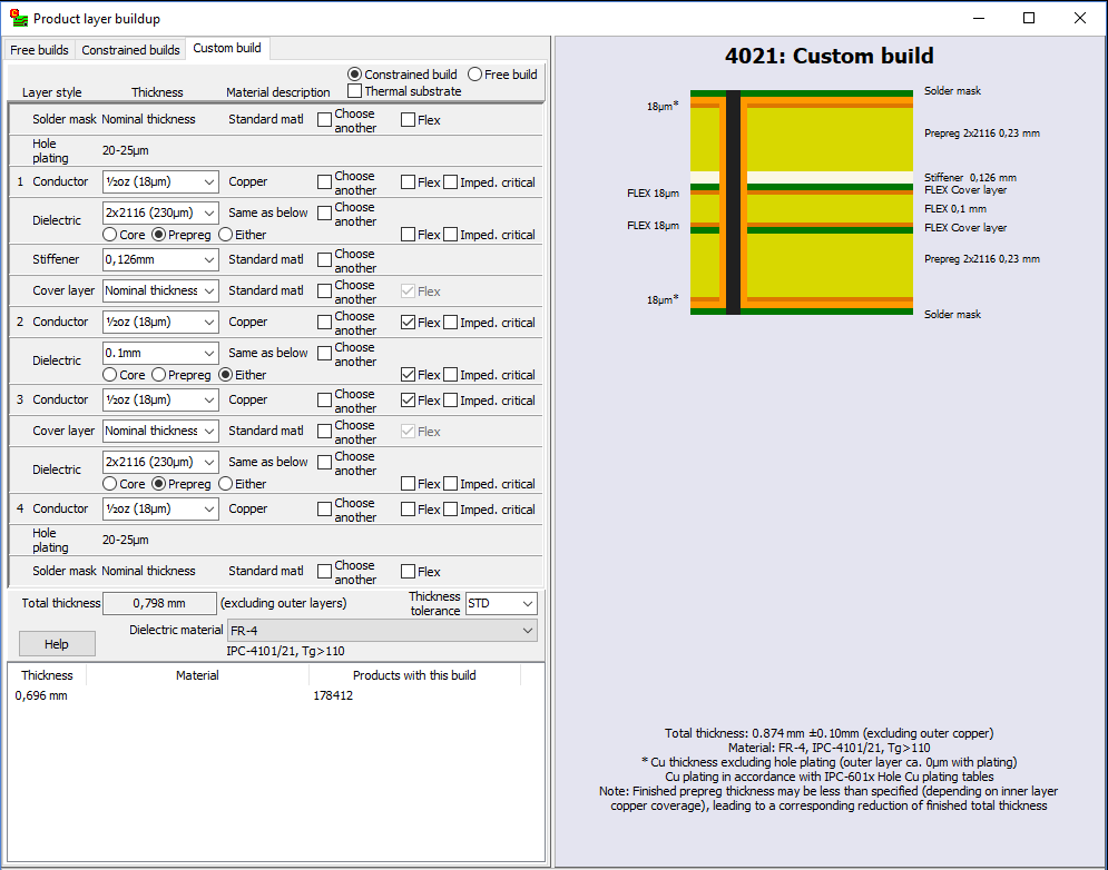
To specify a free custom build, specify the thicknesses for each conductor layer, and specify the total thickness.
To specify a constrained custom build, select or specify a thickness for each layer in the build.
Thicknesses may be selected from the drop down list or entered in the text box. An integer value will be interpreted as µm. A value with a decimal character will be interpreted as mm.
By default, custom builds are symmetric. When first specifying a thickness in the upper half of the build, the same thickness will be applied to the corresponding layer in the lower half of the build. In order for this function properly, all conductor and dielectric thicknesses should be specified before adding other layers to the build. Asymmetric buildups should be avoided, as this can lead to warping and other difficulties during manufacture.
The dielectric material for the build should be selected from the list at the bottom of the frame (to the right of the Help button). A wide variety of commonly used dielectric materials are included in the list. If you require a material that is not in the list, choose User defined (from the bottom of the list) and specify the material. The use of non-standard materials or thicknesses can greatly increase the cost and delivery time of the product.
The standard thickness tolerance is ±10%. Specifying a tighter tolerance will lead to higher costs.
At the bottom of the dialog box, there is a list of previously specified custom builds (if any). Select one of these to reuse the build in the new product.
Conductor layers
Select or specify a thickness for the conductor foil. The specified thickness should not include the thickness of hole plating. Plating is specified as a separate “layer.”
Conductor layers may be marked as flexible.
Conductor layers may be marked as having a thickness which is impedance critical.
By default, conductor layers are copper. To specify special requirements for the layer, check off for Choose another and enter the material name, manufacturer and/or description as desired.To edit the material description, right-click on the layer.
In the rare case where a multi-layer board has an odd number of copper layers, this must be specified by omitting one of the inner copper layers. For example, to specify a 3-layer board you should define a 4-layer build and specify Omit as the copper thickness for one of the inner layers.
Dielectric layers
Select or specify a thickness for the dielectric layer. The thickness of a dielectric layer may also be specified as a combination of prepreg sheets. Prepreg should be specified as follows:
qty x type [+ qty x type [+ qty x type]]
(without any spaces). For example, combinations such as 2x2116 or 1x1080+2x7628 are allowed. Valid prepreg types are 106, 1080, 2112, 2113, 2116, 2125, and 7628. Note: A nominal thickness is used for each prepreg type. The actual thickness may vary slightly depending on manufacturer.
Dielectric layers may be specified as core, prepreg or either. (If the thickness is specified as prepreg sheets, it will automatically be interpreted as prepreg when specified as either.)
Dielectric layers may be marked as flexible.
Dielectric layers may be marked as having a thickness which is impedance critical.
By default, dielectric layers use the material specified at the bottom of the frame (to the right of the Help button). To specify special requirements for the dielectric layer, check off for Choose another and select a material from the drop-down list.
Solder mask layers
Solder mask layers may only be added to the top and/or bottom of the build. Right-click on the desired conductor layer to add a solder mask. You need only add a solder mask layer to the build if you have special requirements.
The thickness may not be specified. Solder mask layers may be marked as flexible.
By default, solder mask layers use the manufacturer’s standard material. To specify special requirements for the layer, check off for Choose another and specify the material. To edit the material description, right-click on the layer.
Cover-layer layers
Cover-layer layers may only be added to conductor layers which are marked as flexible. Right-click on the desired conductor layer to add a cover-layer. You need only add a cover-layer layer to the build if you have special requirements, or for rigid-flex boards.
By default, the thickness is specified as Nominal thickness, which means that the manufacturer will use a suitable thickness. A different thickness may be selected or entered as desired. Cover-layer layers are always marked as flexible.
By default, cover-layer layers use the manufacturer’s standard material. To specify special requirements for the layer, check off for Choose another and specify the material. To edit the material description, right-click on the layer.
Stiffener layers
Stiffener layers may only be added to cover-layer or copper layers which are marked as flexible. Right-click on the desired layer to add a stiffener layer. You need only add a stiffener layer to the build if you have special requirements, or for rigid-flex boards.
By default, the stiffener thickness is calculated to give a total flex+stiffener thickness of 0.30 mm, if possible. A different thickness may be selected or entered as desired. Stiffener layers are not marked as flexible.
By default, stiffener layers use the manufacturer’s standard material. To specify special requirements for the layer, check off for Choose another and specify the material. To edit the material description, right-click on the layer.
Adhesive/bonding layers
Adhesive or bonding layers may be added above or below any layer. Right-click on the desired layer to add an adhesive or bonding layer. You need only add an adhesive or bonding layer to the build if you have special requirements.
By default, the layer thickness is specified as Nominal thickness, which means that the manufacturer will use a suitable thickness. A different thickness may be selected or entered as desired. Manufacturers usually know where and how to best make use of adhesive or bonding layers.
Adhesive or bonding layers may be marked as flexible.
By default, adhesive or bonding layers use the manufacturer’s standard material. To specify special requirements for the layer, check off for Choose another and specify the material. To edit the material description, right-click on the layer.
Plating layers
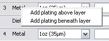 Plating layers represent the presence and thickness of hole plating in the buildup process. They are automatically added to the first and last conductor layer of builds with 2 or more layers. For sequential buildups or buried vias, plating should be added to the inner condcutor layers. To specify this, right-click on the layer and add plating above or beneath the layer (as appropriate). Missing or improperly placed plating layers will affect the display of buried vias in the product stackup drawing.
Note: When specifying plated inner layers, the inner layer (foil) thickness should be specified as 20 μm less than the desired layer thickness.
The plating thickness may not be specified. For IPC Class 1 or 2, plating shall be at least 20 μm thick. For IPC Class 3, plating shall be at least 25 μm thick. (For flexible layers, other rules apply.) Note that actual plating thickness can vary greatly from one place to another on the board, subject to plating process conditions. It is therefore not advisable to use a plated layer for impedance critical signal paths.
Metal-based boards
To specify a stackup for a metal-based board, check off for Thermal substrate (near the top of the frame). For a 2-layer build, you may choose a thermal Core rather than a thermal substrate at the bottom of the build.
Note: For metal-based boards, the material specified at the bottom of the frame (to the right of the Help button) specifies the thermal dielectric. It is not possible to specify special requirements for the dielectric layer(s) adjacent to the thermal substrate or thermal core.