Test fixtures
Test fixtures Bruce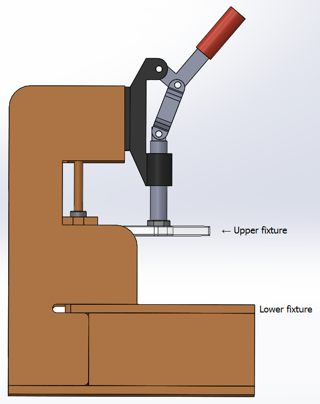 A test jig is an apparatus into which a printed circuit board assembly (PCBA) may be inserted, so that appropriate contacts may be made for in-circuit testing. Typically, the test jig holds the PCBA between an upper and lower test fixture. When the two fixtures are pressed together, ;spring-loaded test pins make contact with test points on the PCBA, thereby allowing test circuitry to perform an in-circuit test of the PCBA.
The Test Fixture Designer module supports designing fixtures for three different generations of test jigs: The Macaos Integrated Test Jig, the Macaos Box Jig, or a legacy jig. You will find the Box and Legacy jigs, as well as a variety of test pins, cables and other accessories, available for purchase from the Global products|Test accessories folder in the Macaos Enterprise Product Browser.
The Test Fixture Designer module imports test pin locations, if they are included in the component layer of the PCBA to be tested.
Note: Do not confuse test points with test pins or test pads.
-
Test pads are the locations for bare-board testing of the PCB during manufacture, which are extracted from an IPC-D-356 file to the Test pads layers.
-
Test points are specific pads or pins on the PCBA which would be used for in-circuit testing. For each test point, a “component” (with the Test point component class) should be added to the appropriate component layer. Ideally, test points (with TPxx designators) should be included in Pick and Place data, but they may also be created manually.
-
Test pins are the pins in a test fixture which will make contact with the PCBA during in-circuit testing.
Supported test jigs
Supported test jigs BruceMacaos Integrated Test Jig
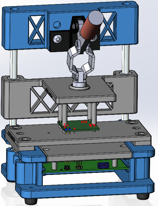 The Macaos Integrated Test Jig is a new design which integrates test circuitry into a modular test jig. It is developed for increased reliability and ease of design, compared to the Box Jig or the Legacy Jigs.
A PCB with test circuitry is located in the base of the jig, and the test pins are soldered into this PCB.
The user selects an active area size, and then specifies the locations and types of Guide Pins and Test Pins. From this information, the Upper Fixture, Protective Cover and Receptacle Plate (the three gray modules shown at the right) are generated and added to the jig. In addition, a Gerber file with the pin locations and profile of the Test Circuitry PCB is automatically generated.
The fixture specifications (in mm) are:
| Active test area width (X-dimension) | 80/100/120/140/160/180 |
|---|---|
| Active test area depth (Y-dimension) | 60/70/80/90/100/110/120/130/140/150 |
| Test electronics PCB width (X-dimension) | Active test area width + 20 |
| Test electronics PCB depth (Y-dimension) | Active test area depth + 40 |
| Clearance above/below PCBA under test | 34/4.5 |
| Clearance above/below test circuitry PCB | 12/33 |
| Test circuitry PCB thickness | 1.6 |
Macaos Box Jig
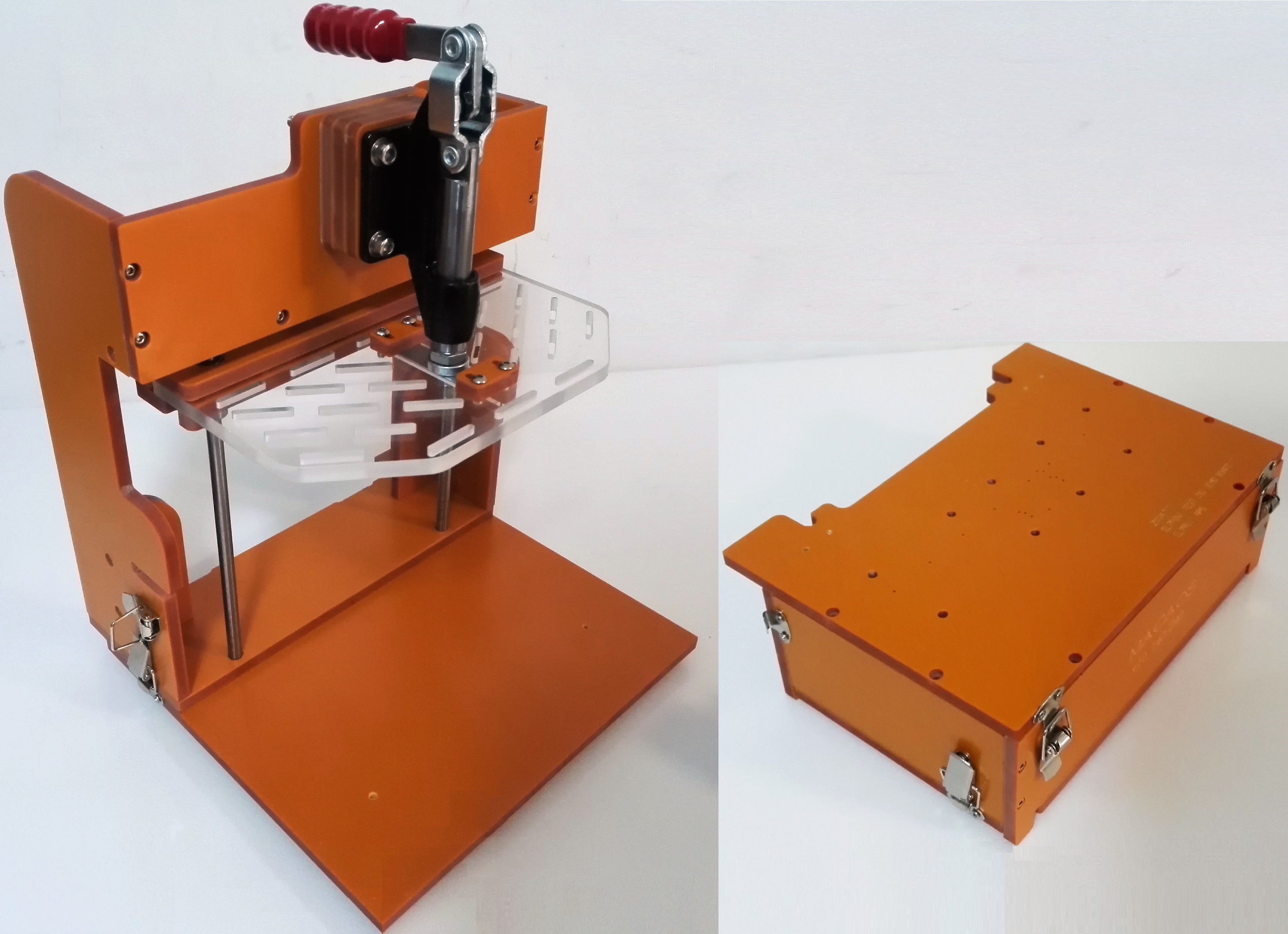 The Macaos Box Jig is a test jig where the lower fixture is a box deep enough to contain test electronics, as well as connectors mounted in the side walls. Both the top and bottom of the lower fixture box are hinged, in order to give easy and flexible access.
The standard lower fixture has holes drilled for the test pin receptacles.
An alternative is to have a large opening in the lower fixture, over which a PCB is placed. In this case, a Gerber file specifying the board outline, mounting holes and test pin locations is generated. This Gerber file may be imported to a CAD system for designing the PCB.
The jig is supplied with an upper fixture. This fixture has slots for placing press pins as needed to insure good contact between the PCBA and the test pins in the lower fixture.
In the Macaos Box jig, both fixtures are easily replaced. The lower fixture is held in place with two latches. The upper fixture is held in place with two thumbscrews and a magnet.
The fixture specifications (in mm) are:
| Fixture type | Lower | Lower w/PCB | Upper |
|---|---|---|---|
| Active area width (X-dimension) | 240 | 70–240 | 240 |
| Active area depth (Y-dimension) | 140 | 70–140 | 140 |
| Fixture width (X-dimension) | 260–500 | 300–500 | 240 |
| Fixture depth (Y-dimension) | 160–500 | 160–500 | 60–500 |
| Fixture height/thickness (Z-dimension) | 91 | 91 | 8 |
Legacy Jig
 The Legacy Jig is a simple test jig, where the lower fixture is attached to a deep base. With the legacy fixture, the “box” is part of the jig (rather than part of the fixture, as with the Box Jig). The Legacy Jig is available in three sizes.
The lower fixture may be a single plate or a box which fastens onto the jig base.
The jig is supplied with an upper fixture. This fixture has slots for placing press pins as needed to insure good contact between the PCBA and the test pins in the lower fixture.
The fixture specifications (in mm) are:
| Fixture type | Lower (flat) | Lower (box) | Upper |
|---|---|---|---|
| Active area width (X-dimension) | 120/200/260 | 120/200/260 | 120/200/260 |
| Active area depth (Y-dimension) | 80/120/150 | 80/120/150 | 80/120/150 |
| Fixture width (X-dimension) | 160/240/300 | 170/260/320 | 160/155 or 216/364 |
| Fixture depth (Y-dimension) | 100/140/170 | 108/150/180 | up to 500 |
| Fixture height/thickness (Z-dimension) | 8 (2–20) | 33 (33–100) | 8 (2–20) |
Custom size
A custom size fixture may be designed for use with other test jigs.
The fixture specifications (in mm) are:
| Fixture type | Lower (flat) | Lower (box) | Upper |
|---|---|---|---|
| Active area width (X-dimension) | 0–500 | 0–500 | 0–500 |
| Active area depth (Y-dimension) | 0–500 | 0–500 | 0–500 |
| Fixture width (X-dimension) | 0–500 | 0–500 | 0–500 |
| Fixture depth (Y-dimension) | 0–500 | 0–500 | 0–500 |
| Fixture height/thickness (Z-dimension) | 8 (2–20) | 33 (33–100) | 8 (2–20) |
Test fixture
Test fixture BruceA test fixture has a top surface with holes where test pin receptacles and guide pins may be inserted. At each test pin point, a pin receptacle is inserted. A spring-loaded test pin (or Pogopin) is then inserted into each receptacle so that it will make contact with desired test point on the PCBA. The PCBA is placed on top of the pins and then pressed down so that the pins make good contact with the test points.
The Macaos Integrated Test Jig includes a lower test fixture with pins and receptacles inserted. Fixture plates for the Box or Legacy jigs are supplied without pins or receptacles. For these jigs, you will need to acquire and insert appropriate pins and receptacles into the test fixture plate.
Ideally, all test points should be accessible to the lower test fixture. The Macaos Integrated Test Jig does not support test points on both sides. However, for the Box or Legacy jigs, a PCBA-specific upper fixture may be designed, if necessary.
 Macaos Integrated Test Jig
The Macaos Integrated Test Jig incorporates an upper press fixture, a protective cover, a receptacle plate, and a test circuitry PCB. This is delivered fully assembled, with pins/receptacles installed.
To insure stability and compatibility, only P100/R100 and PL75/RL75 pins and receptacles are supported. When defining test points, the desired pin head style must be specified. It is also necessary to specify suitable locations for guide/support pins. (Press pins are placed at the guide/support pin locations.)
Use the Gerber button to generate a Gerber file of the test circuitry PCB outline and pin locations, for import to your CAD system. Connectors and indicators may be placed at the front and/or back edge of the PCB.
Note: The Integrated test jig does not support test points on both sides of the PCBA.
Macaos Box test jigs
With the Macaos Standard test jig, the lower fixture is a box, in which test circuitry may be installed as desired. The box height is always 91 mm, but its width and depth may be expanded as necessary. Connectors may be mounted in the sides or top of the box. This jig supports three fixture styles:
-
Lower fixture: The top surface of the box has holes for test pin receptacles and guide pins.
-
Lower w/ PCB fixture: The top surface of the box has a 240x140 mm opening, over which a PCB with test pin receptacles and guide pins is laid. We recommend a 3.2 mm thick PCB. Use the Gerber button to generate a Gerber file of the PCB outliine and pin locations for import to your CAD system.
-
Upper: An upper fixture has holes for test pin receptacles that will hold the test pins which make contact with the upper side of the PCB.
Legacy jigs
Legacy jigs are early versions of the Macaos test jig. They have a fixed box size and active area. The lower fixture rests on top of the jig box. These jigs support three fixture styles:
-
Lower – box: The lower fixture is a box where connectors may be mounted in the side walls. The top surface of the box has holes for test pin receptacles and guide pins.
-
Lower – flat: The fixture is a plate with holes for test pin receptacles and guide pins.
Alternatively, the fixture may be a PCB in which test pin receptacles and guide pins are installed. We recommend a 3.2 mm thick PCB. Use the Gerber button to generate a Gerber file of the PCB for import to your CAD system. -
Upper: An upper fixture has holes for test pin receptacles that will hold the test pins which make contact with the upper side of the PCB. For the 12/20 jig, two widths of upper fixtures are supported.
Test fixture protective cover
A box or legacy test fixture may be supplied with a protective cover. This is an additional plate (same material as the fixture) with holes drilled to allow all of the test pins to pass through it. Support pins hold the protective cover up, so that all of the test pins are “hidden” in the holes of the protective cover. When the test jig handle is pressed down, the protective cover is pushed down and the test pins make contact with the PCBA.
Test pins
Test pins Bruce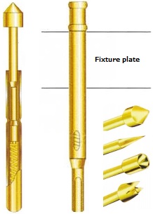 Test pins are available with a variety of different heads, depending on the type of pad, solder joint or component pin they are to make contact with.
For the Macaos Integrated Test Jig, the desired head must be specified for each test point. The jig is supplied fully assembled, with pins inserted into receptacles, which are soldered to the test circuitry PCB.
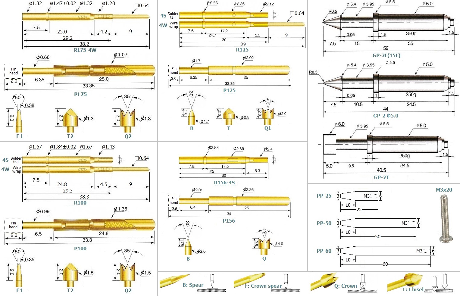
The most commonly used pin heads are:
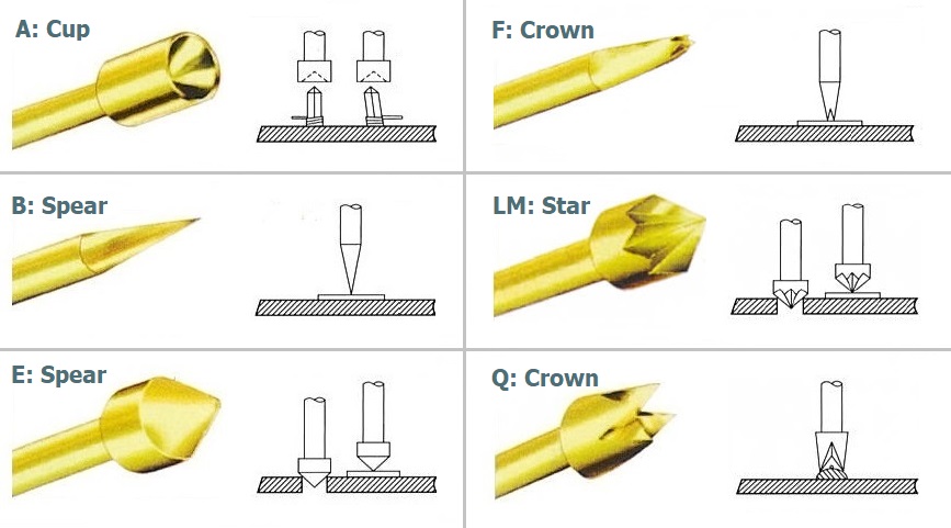
As shown, it is important to choose a pin head suitable for contact with the test point on the PCBA.
For the Box and Legacy jigs, the user must insert appropriate pins and receptacles into the fixture plate(s), and connect or solder them to their test circuitry. The Macaos Test Jig Starter Kit contains a variety of pins, receptacles, connectors, etc for this purpose.
Note: For best results, all test pins in a fixture should have approximately the same height above the fixture plate, both when fully extended and fully depressed. In the Macaos assortment, types PA50/R50 and P75/R75 are compatible with each other. In the same manner, types PL75/RL75, PA100/R100, PA125/R125 and PA156/R156 are compatible. Other combinations (such as mixing PA50/R50 with PA100/R100) are NOT recommended.
A variety of test pins are available for purchase in the Test accessories folder of the Product browser.
Macaos Test Jig Starter Kit
The Macaos test jig starter kit includes the following pins, receptacles and accessories:
Creating a Macaos Integrated Test Jig and fixture
Creating a Macaos Integrated Test Jig and fixture BruceSelect a PCB product or test fixture and then click on the Test Fixture button to open the Test Fixture Designer module.
Creating a Macaos Integrated Test Jig test fixture involves several steps:
-
Select Macaos Integrated Test Jig as the test jig style. If necessary, adjust the active area, and then click on the Redraw fixture button to view the fixture and jig. The active area is displayed as a rounded rectangle, drawn with a thick line.
-
Use the blue Rotate and Offset buttons to place the board within the active area, as necessary. The board should be placed so that all test pins will be within the active area, and that the centroid of the test pins will be near the center of the active area.
The board offset buttons move the board right or up 10mm per click. If you press the Shift key, then the board will move 1mm per click.
Note: If all of your test points are on the top side of the PCB, you may use the blue Flip button to turn the PCB upside-down in the test fixture editor. This mirrors the board, and allows placing test pins at pads on the copper top layer (rather than the copper bottom layer).
-
If desired, annotation text may be added to the fixture. Enter the desired text in the Text to place edit box, select a rotation, and click on the Place text button (so that it is down). Then click at the desired location to place the text. Right-click on the edit box to load texts such as the product number or company name.
To delete text, click on the Delete text button (so that it is down) and then draw a selection rectangle around the text to delete.
-
Go to the Pins tab. If test points (components with Test point class) have been defined in the (Assembly Data Manager) on a component layer, they may be imported as test pins. See point 7 below for a description of the test pin parameters.
-
Support pins for the test circuitry PCB are automatically added near each corner of the PCB. Note: Two of these pins are within the active area. If they are in conflict with test point locations, they must be deleted and manually placed at a suitable location. To do so, select Support/switch as the type of pin to place and choose Test circuitry support pin, click on the Place pins button (so that it is down) and then click at an appropriate location.
-
Click on the Place pins button (so that it is down). Integrated Guide pins must be added at holes with at least 1.0 mm diameter. If holes are not available, then Integrated Edge Guide pins may be placed along the board edges, Integrated Support pins must be placed at suitable locations under the PCBA. There should be at least 4 guide/support pins.
-
Place test pins at the appropriate test points. Select Test as the type of pin to place, choose a pin receptacle, and then click on the Place pins button (so that it is down). Then click at the desired location to place the pin.
Note: The standard pin receptacle is R100, which is suitable for 2.54 mm center-to-center spacing. If necessary, the R75 receptacle (for 1.91 mm spacing) may also be used. Receptacles for smaller spacing are not available for the Macaos Integrated Test Jig.
When placing a test pin, the following should be specified:
- Designator and pin number (recommended)
- Signal name (recommended)
- External connector pin (optional)
- Test pin head style (required)
This information is used to generate a wiring list for the test fixture and to insert the proper test pin into each receptacle.
Although not recommended, the pin location and/or hole diameter may also be modified.
Note: The minimum allowed edge-to-edge spacing between receptacle holes is 0.4mm
To edit a test pin, right-click on the pin in the list. Guide/support pins are not normally shown in the list. Right-click and choose Show guide pins in list to make them visible.
To delete pins, click on the Delete pins button (so that it is down) and then draw a selection rectangle around the pins to delete.
-
As test pins are added to the fixture, the centroid of the test pins is shown as a hexagon. The press point will be adjusted to be near the centroid when the test jig is assembled.
-
If desired, specify the location of the activation push button switch, which may be used to activate the test circuitry when the test pins have made contact with the test points on the PCB under test. A post will push the button when the jig is in the lower position.
Select Support/switch as the type of pin to place, choose Activation switch, click on the Place pins button (so that it is down) and then click at an appropriate location. The switch should be placed near the edge of the active area, at a position which does not conflict with any test pins.
-
Note: If desired, you may go to the Z-axis tab to view the vertical configuration. However, since the Macaos Integrated Test Jig is delivered fully assembled, this is not strictly necessary.
- When you are finished placing pins, click on the Publish button to publish the test fixture product to the Product Browser. While publishing, you will be asked to attach a STEP (3D model) file of the PCBA under test. We strongly recommend that this file be included, as this will help prevent conflicts between the components on the PCBA and the test fixture/jig.
-
Use the Gerber or DXF button to generate a Gerber or DXF file which contains:
-
The outline of the test circuitry PCB.
-
1.3 mm pads, which indicate the test pin locations. On the test circuitry PCB, these should be 1.3 mm plated holes with appropriate padstacks. In a Gerber file, each test pin location is annotated with the Des:Pin of the test point.
-
3.2 mm pads, which indicate the support pin locations. On the test circuitry PCB, these should be 3.2 mm non-plated holes. In a Gerber file, each pin location is annotated with the letter C.
-
A 6.5 mm square, 1.25 mm circle and 0.5 mm pad. In a Gerber file, this is annotated with the letter A. The 0.5 mm pad indicates where the center of the activation switch should be placed on the test circuitry PCB. The square and circle provide a graphical representation of the switch outline and the pushbutton. The switch should be an Omron B3SL-1002P or B3SL-1005P (or similar). See https://omronfs.omron.com/en_US/ecb/products/pdf/en-b3sl.pdf
This Gerber or DXF file may be imported into your CAD system as a guide for development of the test circuitry PCB. The Macaos Integrated Test Jig is supplied with all test pins and receptacles inserted into the jig’s receptacle plate. The receptacle plate may be easily removed from the jig for attachment of the test circuitry PCB to it.
-
Creating a test fixture for other test Jig styles
Creating a test fixture for other test Jig styles BruceSelect a PCB product or test fixture and then click on the Test Fixture button to open the Test Fixture Designer module.
If a test fixture already exists for the selected PCB product, you may choose to create a matching opposite side fixture; which will have the same press point and board locations. Otherwise, you must choose a test jig size and a fixture style. Note: If a test fixture was selected when opening the module, then a matching fixture will be created.
Creating a test fixture in Macaos Enterprise involves several steps:
-
Select a test jig style and fixture style. Select or specify a fixture material and other dimensions, as appropriate. Set a check mark if you wish a protective cover.
-
Click on the Redraw fixture button to view the fixture and jig.
-
If desired, annotation text may be added to the fixture plate. Enter the desired text in the Text to place edit box, select a rotation, and click on the Place text button (so that it is down). Then click at the desired location to place the text. Right-click on the edit box to load texts such as the product number or company name.
To delete text, click on the Delete text button (so that it is down) and then draw a selection rectangle around the text to delete.
-
If you have chosen a box-style fixture, then you may place connector openings in the side walls of the fixture. Select a connector style and click on the Place connector button (so that it is down). Then click at the desired location within the fixture top plate or any of the side walls.
If large enough, the connector name is displayed inside the opening for the connector body. To change the connector name, right-click on the connector in the list and select Change connector description.
To delete a connector, right-click on the connector and select Delete.
-
The piston offset should be set to the actual position of the handle piston of the test jig. (For the Macaos standard jig, this would be 32mm plus 8mm for each spacer plate used when mounting the handle on the jig.) Use the green Offset buttons to adjust the piston offset from the back edge of the active area. The press point offset buttons will move the press point down or up 10mm per click. If you press the Shift key, then the press point will move 1mm per click.
-
Use the blue Rotate and Offset buttons to place the board within the active area, as necessary. The board offset buttons move the board right or up 10mm per click. If you press the Shift key, then the board will move 1mm per click.
Note: If all of your test points are on the top side of the PCB, you may use the blue Flip button to turn the PCB upside-down in the test fixture editor. This mirrors the board, and allows placing test pins at pads on the copper top layer (rather than the copper bottom layer).
-
To place pins, go to the Pins tab. Select the type of pin to place and click on the Place pins button (so that it is down). Then click at the desired location to place the pin.
- Press/support pins may be placed at any location.
- Guide pins (used to align the PCBA on the fixture) may only be placed at a hole of suitable diameter.
- Edge guide pins may be placed at any location along the edge of the PCB. A hole with the specified diameter will be placed one pin radius from the board edge.
- Test pins may be placed at any hole or pad.
If test points (components with Test point class) have been defined (in the Assembly Data Manager) on a component layer, they may be imported as test pins.
When placing a test pin, the following should be specified:
- Designator and pin number (recommended)
- Signal name (recommended)
- External connector pin (optional)
- Test pin head style (optional)
The signal name and connector pin number are used to generate a wiring list for the test fixture.
Although this is not recommended, you may also modify the pin location and/or hole diameter, if desired.
Note: The minimum allowed edge-to-edge spacing between pin holes is 0.4mm
To edit a test pin, right-click on the pin in the list. Guide/support/press pins are not normally shown in the list. Right-click on the list and choose Show guide pins in list to make them visible.
To delete pins, click on the Delete pins button (so that it is down) and then draw a selection rectangle around the pins to delete.
-
Ideally, the press point should be located over the centroid (geometric center) of the fixture pins. Click on the Centroid button to move the board so that the pin centroid is aligned with the press point. Note: If pins fall outside of the active area or test fixture, then you will need to adjust the press point offset and/or adjust the position of the board. (If you change the press point offset, then you may also need to click on the Centroid button again.)
-
Go to the Z-axis tab to check the z-axis spacing for the jig and fixture. Specify the dimensions as necessary, and select guide pin and test pin types. Use the radio buttons to view spacing with the jig handle up and down.
When the handle is down, if there is too little or too much spacing between the fixture plate and the PCBA, then a warning message is displayed in the diagram.
Note: Test pin dimensions are based on the test pin connecting to the surface of the PCBA. In cases where the test pin will contact a solder bump or component lead some extra space will be needed. It is therefore advisable to have 1-2mm of deflection space available when the handle is down.
Note: The most recent view of each Z-axis diagram (handle up and handle down) will be included with the fixture data when the fixture is published. If you do not view a diagram, then it will not be included.
- When you are finished placing pins and positioning the press foot and board, click on the Publish button to publish the test fixture product to the Product browser. This generates a drill file for the fixture plate, as well as a wiring list and documentation.
-
When creating a test fixture as a PCB, use the Gerber or DXF button to generate a Gerber or DXF file which contains the outline of the test circuitry PCB as well as pads indicating the location and diameter of holes in the test circuitry PCB.
-
A pad annotated with the letter G represents the location and diameter of a non-plated hole for a guide pin. Note: Pads are not annotated in a DXF file
-
A pad annotated with the letter S represents the location and diameter of a non-plated hole for a support pin. Note: Pads are not annotated in a DXF file
-
All remaining pads represent the locations and diameters of holes for a test pin receptacles. On the test circuitry PCB, these should be plated holes with appropriate padstacks. In a Gerber file, each test pin location is annotated with the Des:Pin of the test point.
This Gerber or DXF file may be imported into your CAD system as a guide for development of the test circuitry PCB.
-
After the fixture product has been published, the Operations|Print|Documentation set command will create a PDF file listing the product parameters and wiring list, together with a drawing which shows the location of each test pin.
Saving a work in progress
Saving a work in progress BruceSaving a work in progress
It is possible to temporarily save a partially designed test fixture. Click on the Save button to save your work. To reload, first select the PCB and open the test fixture creator. Then click on the Load button to load the temporary test fixture file.
Tips and tricks
Tips and tricks BruceIf you have bare-board test pad data (in IPC-D-356 format) available for the PCB under test, this should be imported to the product prior to creating a test fixture. Test pad data can either be imported when the product is initially created in the Import module, or it can be imported to an existing product in the Assembly Data Manager. Each time a test pin is created, if a test pad exists at that location then the signal name, designator and pin number will automatically be extracted from the test pad for use with the test pin being created.
As pins are added to a test fixture, information is added to three “layers”:
-
A pad with the hole diameter is added to the Test fixture lower or Test fixture upper layer.
-
A symbol and text are added to the Test fixture drawing layer. For test pins the symbol represents the receptacle style: ▼ = R50, × = R75, + = R100, □ = R125, ▲ = R156, and the text indicates the pin head style (if specified). For other pins, the symbol is a large cross, and the text is: G = guide pin, S = support pin, P = press pin, C = test circuitry support pin. For an activation switch, the symbol is a square surrounding a circle, with the letter A.
-
For test pins only, a cross and the Des:Pin or Signal name text are added to the Test fixture annotation layer.
Macaos Integrated Test Jig
For best results, a PCBA under test should be rotated so that the long dimension is the X dimension.
Box and legacy jigs
Test pins with different diameters usually also have different heights. Types R50 and R75 are of similar height and may be used together. Types RL75, R100, R125 and R156 are also of similar height and may be used together. Other combinations are not recommended.
The Macaos test accessories include cables that mate to test pin receptacles with wire-wrap bases. However, it may be difficult to attach connectors to all pins in a tight 1.91 pitch array. Therefore, we recommend avoiding a large number of tightly spaced test pins.
Guide pins are designed for use with a bottom side fixture. They must be located at appropriate holes in the board. These both align and support the board. To provide support for the board in an area without suitable holes, a support pin may be placed. These have a flat top and are shorter than guide pins.
Macaos Box and Legacy jigs are supplied with a universal top fixture with numerous slots, allowing press pins to be placed where appropriate. It will normally only be necessary to make a top-side fixture if it is not possible to access all test points from one side of the board.
If you wish to create test fixtures for testing two or more PCBs at the same time, you can create Multi-product panels with the PCBs to be tested, and then create a test fixture for the panel.