Solder pallets
Solder pallets BruceThere are two styles of solder pallets:
-
A wave solder pallet exposes the entire solder side of the PCB to the solder wave. For panels, there is an opening for each board in the panel. This would typically be used to support small, thin or irregularly shaped PCBs as they travel through the wave soldering machine.
-
A selective wave solder pallet exposes only regions with plated through-hole (PTH) components to the solder wave, while protecting other regions from the solder wave. This would typically be used when soldering PTH components on a board which also has surface-mounted (SMT) components, gold fingers, ground planes, heat-sensitive or other areas needing protection on the solder side of the PCB.
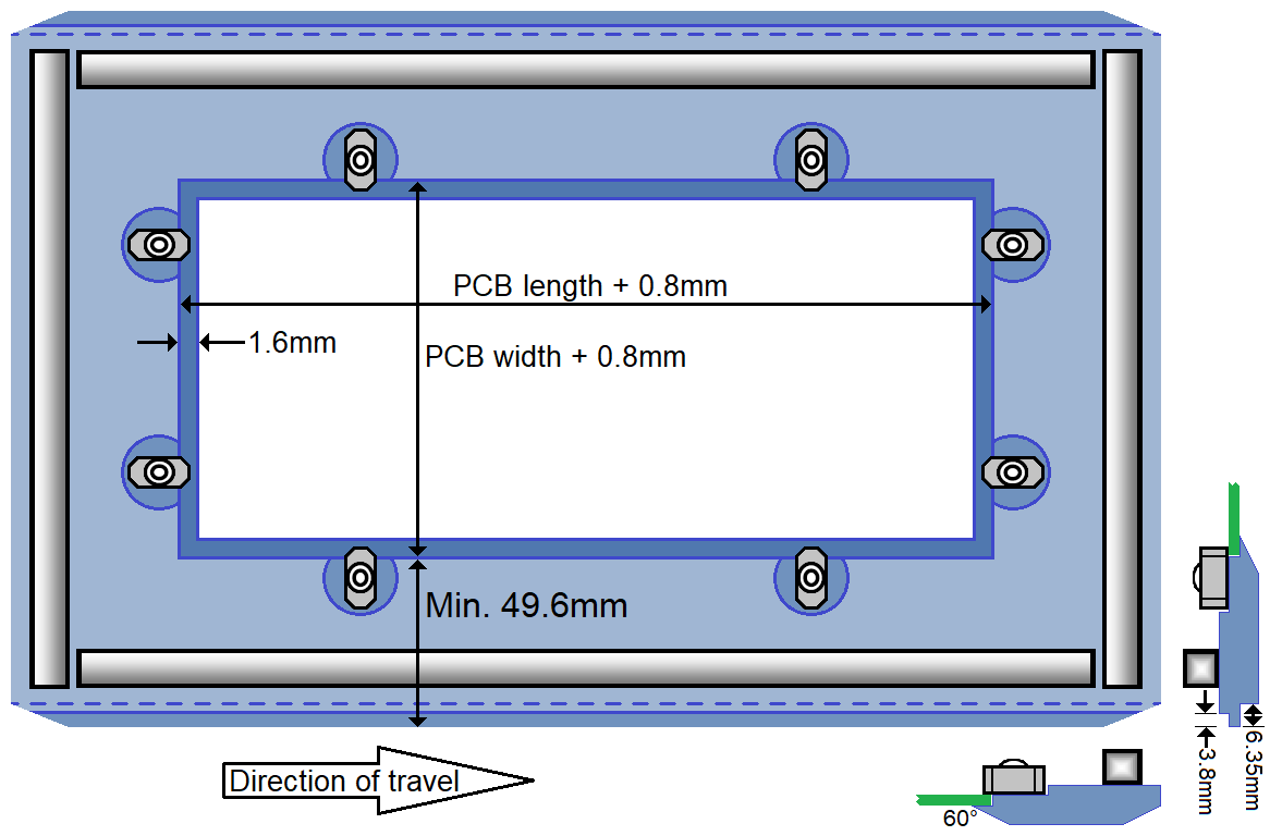
Both styles of wave solder pallets have the same frame, with stiffener/solder-dam on all four edges of the top side, and rotary PCB fasteners. The bottom edge of the rail fingers is flush with the bottom side of the PCB. The leading and trailing edges, as well as all four corners, are chamfered.
In Macaos much of the pallet design is calculated automatically. You need only define the following:
-
outer dimensions and material parameters
-
placement of PCB fasteners
-
solder wave openings (selective wave solder pallets only)
-
component pockets (selective wave solder pallets only)
Your input is welcome
The pallet creator is a new module in Macaos Enterprise. Although we have done our best to develop a module that is both fully functional and easy to use, there are undoubtedly things we haven’t thought of. If you have suggestions or wishes for improving this module, we welcome your input. Please send your feedback to support@macaos.com.
Creating a wave solder pallet
Creating a wave solder pallet Bruce-
Select pallet style. Upon starting the pallet designer module, select the Wave solder pallet style.
-
Specify board placement. The board is placed in the center of the pallet with top side up. If desired, you may rotate or flip the board by clicking on the appropriate button in the Placement tool bar.
-
Specify pallet properties. Specify the product name, article and description. Adjust the pallet dimensions, if necessary. Select a pallet material and thickness. Check that the PCB thickness is correct. If the board does not require a lead-free soldering process, remove the Pb-Free check mark.
-
Place board fasteners. Specify the length (from pivot-point to end) of the fasteners, and how much they should overlap the board edges. Then click on the Place button (so that it is down). Click and drag the circle to the desired location, then release the mouse button to place a fastener. Repeat as necessary.
If you need to delete a fastener, click on the Delete button (so that it is down). Draw a selection rectangle around the entire fastener and circle that you wish to delete.
-
Generate a milling file. If desired, a milling file may be generated. The milling file(s) may be used to make the pallet with your own milling machine. Click on the Save button to save the milling file in G-Code format. After specifying a file name, the Milling program setup dialog box is used to specify the necessary parameters to generate an output file with the correct coordinates and operating commands for the target milling machine.
-
Publish the pallet product. Upload the pallet to the Macaos Repository. It may then be reopened for modification or to generate a milling file. It is also possible to purchase a finished pallet product (with stiffeners and fasteners).
Note: When creating a pallet for a panel which has not been created with the Macaos Enterprise panelization module (as well as for some older panels), solder openings for the individual boards in the panel will not be automatically defined. In these cases, the opening outlines must be defined by the user. See step 5 in the next section for details.
Creating a selective wave solder pallet
Creating a selective wave solder pallet Bruce-
Select pallet style. Upon starting the pallet designer module, select the Selective wave solder pallet style.
-
Specify board placement. The board is placed in the center of the pallet with top side up. If desired, you may rotate or flip the board by clicking on the appropriate button in the Placement tool bar.
-
Specify pallet properties. Specify the product name, article and description. Adjust the pallet dimensions, if necessary. Select a pallet material and thickness. Check that the PCB thickness is correct. If the board does not require a lead-free soldering process, remove the Pb-Free check mark. Specify pocket depths for solder-side component pockets.
-
Place board fasteners. Specify the length (from pivot-point to end) of the fasteners, and how much they should overlap the board edges. Then click on the Place button (so that it is down). Click and drag the circle to the desired location, then release the mouse button to place a fastener. Repeat as necessary.
If you need to delete a fastener, click on the Delete button (so that it is down). Draw a selection rectangle around the entire fastener and circle that you wish to delete.
-
Specify openings in the pallet. Select Pallet opening as the active layer. Select one of the three drawing modes to draw the boundary of the opening.
- Draw rectangle: Click at one corner of the rectangle, then drag the mouse pointer to the opposite corner and release.
- Draw outline: Click at one vertex of the outline, drag the mouse pointer to the next vertex and release the mouse button. Click and drag to each additional vertex of the outline. All edges automatically snap to orthogonal or diagonal. To close the outline, press the F9, Space or Return key. To abort creation of the outline, press the Esc key.
- Draw orthogonal outline: Use the same technique as for drawing an outline. All edges automatically snap to orthogonal.
To delete an outline, click on the Delete button (so that it is down). Draw a selection rectangle around the entire outline that you wish to delete.
 Keep the following rules in mind while defining pallet openings:
- Minimum clearance between the edges of pallet openings and PTH pads is 1.24 mm for PbSn soldering or 2.5 mm for lead-free soldering.
- Aspect ratio guidelines must be followed.
Note: When working with a (single-product) panel which has been created with the Macaos panelization module, the first board in the panel is highlighted with a yellow rectangle. Openings and pockets specified within this rectangle will automatically be copied to all other boards in the panel.
-
Specify pockets. Repeat the process of step 5 for component pockets, as necessary.
 Keep the following clearance rules in mind while defining component pockets:
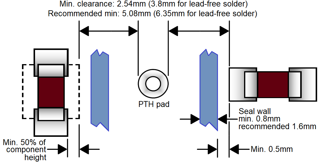
- Minimum 0.8 mm clearance between pocket edges and the edges of pallet openings.
- Minimum 0.5 mm clearance between component and pocket floor.
- Minimum 0.5 mm clearance between pocket edge and component pad, when component is perpendicular to pocket edge. When component is parallel to pocket edge, the minimum clearance is increased by 50% of the component height.
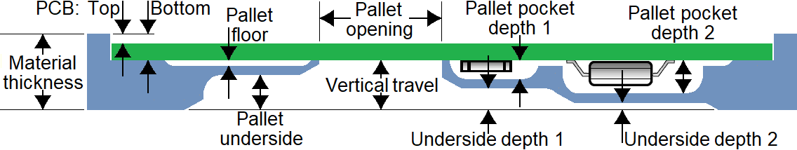
Note: The pallet floor (0.5mm clearance under the PCB) is defined automatically based on the PCB outline and the pallet openings. Likewise, pressure relief regions (on the bottom side) are defined automatically based on the pallet openings and component pockets.
Note: If a pocket is drawn too close to an opening, it will automatically be clipped to give a 0.8 mm clearance between the pocket and the opening.
-
Generate a milling file. If desired, a milling file may be generated. The milling file(s) may be used to make the pallet with your own milling machine. Click on the Save button to save the milling file in G-Code format. After specifying a file name, the Milling program setup dialog box is used to specify the necessary parameters to generate an output file with the correct coordinates and operating commands for the target milling machine.
-
Publish the pallet product. Upload the pallet to the Macaos Repository. It may then be reopened for modification or to generate a milling file. It is also possible to purchase a finished pallet product (with stiffeners and fasteners).
Design guidelines for selective wave soldering
Design guidelines for selective wave soldering Bruce-
Placement: PTH components should, to the extent possible, be placed together. They should be placed far enough from solder-side SMT components to meet the clearance and aspect ratio requirements shown below.
Long PTH components should be placed parallel to the direction of travel over the solder wave. Allow space between long components to close the opening in the solder pallet, in order to increase the strength and functionality of the seal wall and pallet floor.
Do not place SMT components within PTH land patterns. Avoid placing taller SMT components close to PTH components.
-
Clearance: In order to insure sufficient space for the solder wave to adequately solder the plated through-hole, the clearance between PTH pads and SMT pads must meet the minimums shown here. Note that lead-free solder waves require a larger clearance.
-
Aspect ratio: Openings in the wave solder pallet must be large enough for the wave to enter with sufficient pressure to apply solder. Placing taller SMT components farther away from the opening, allows the pallet floor to be “lifted,” thereby improving solder wave pressure.
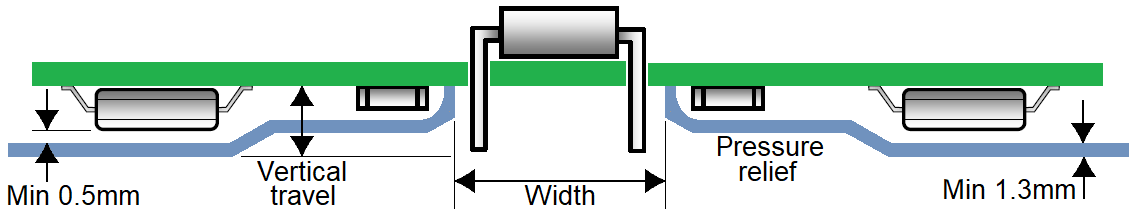
The aspect ratio is defined as opening width / vertical travel, where the width is the dimension perpendicular to the direction of travel. For PbSn soldering, the minimum aspect ratio is 1.0 while for lead-free soldering it is 1.7, as shown in the table below.
Vertical travel SnPb solder Pb-free solder ≤3.8 mm 3.8 mm 6.35 mm 5 mm 5 mm 8.5 mm 6 mm 6 mm 10.2 mm 7 mm 7 mm 11.9 mm 8.15 mm 8.15 mm 13.85 mm The minimum opening width is 3.8 mm for PbSn soldering and 6.35 mm for lead-free soldering, even if the vertical travel is less than 3.8 mm.
If the opening width is less than 7.6 mm then the opening length (parallel to direction of travel) should be at least 3 times the width. For larger widths, the length should be at least as large as the width.
-
Vertical travel: The minimum clearance between the PCB/components and the pallet floor is 0.5 mm. The minimum floor thickness is 1.3 mm. The maximum allowed vertical travel is 8.15 mm, giving a maximum component height of 6.35 mm.
Materials overview
Materials overview BruceThere are four categories of wave solder pallet materials. When creating a pallet, you may specify a category or a specific material. If you specify a category, the manufacturer will select a suitable material from that category.
A flux-resistant material is recommended for use when the solder flux is corrosive, containing halides or dicarboxylic acids.
A high-temperature material is recommended for use when the solder bath temperature exceeds 265°C and the bottom side pre-heat temperature exceeds 140°C.
|
Category |
Economy |
Antistatic |
Optical |
Flux-resistant |
||||
|
Material |
Röchling |
VonRoll |
Haysite |
Röchling |
VonRoll |
Röchling |
Röchling |
VonRoll |
|
Anti-static |
|
Yes |
Yes |
Yes |
Yes |
Yes |
Yes |
Yes |
|
IR-reflective |
|
|
|
|
|
Yes |
|
Yes |
|
Flux-resistant |
|
|
|
|
|
|
Yes |
Yes |
|
High-temperature |
|
Yes |
|
|
|
|
Yes |
Yes |
|
Short-run |
|
Yes |
|
|
|
|
|
|
|
Color |
Blue |
Black |
Black |
Black |
Black |
Grey |
Red |
Grey |
|
Density (g/cm³) |
1.9 |
1.9 |
1.83 |
1.9 |
1.9 |
1.9 |
1.8 |
1.9 |
|
Flex strength 23° (MPa) |
360 |
400 |
187 |
360 |
350 |
360 |
380 |
350 |
|
Flex strength 150° (MPa) |
180 |
220 |
42 |
180 |
|
180 |
260 |
200 |
|
Flex strength 185° (MPa) |
|
80 |
|
|
80 |
|
150 |
|
|
Mod. elasticity 23° (MPa) |
18 000 |
20 000 |
10 500 |
18 000 |
18 000 |
18 000 |
18 000 |
18 000 |
|
Mod. elasticity 150° (MPa) |
9 000 |
14 000 |
4 000 |
9 000 |
|
9 000 |
14 000 |
12 000 |
|
Mod. elasticity 185° (MPa) |
|
7 800 |
|
|
6 000 |
|
10 000 |
|
|
Water absorption (%) |
<0.20 |
<0.15 |
0.16 |
<0.20 |
0.15 |
<0.20 |
<0.20 |
<0.10 |
|
Coef linear expan. (10-6/°K) |
13 |
|
11.5 |
11 |
10.1 |
11 |
11 |
10.1 |
|
Thermal cond. (W/m°K) |
0.25 |
|
0.425 |
0.25 |
0.3 |
0.25 |
0.23 |
0.3 |
|
Std operating temp (°C) |
260 |
300 |
300 |
260 |
260 |
260 |
300 |
300 |
|
Max operating temp (°C) |
300 |
|
|
300 |
350 |
300 |
380 |
350 |
|
Surface resistivity (ohms) |
|
105-109 |
105-109 |
105-109 |
105-109 |
105-109 |
105-109 |
105-109 |
Milling details
Milling details BruceThe pallet is milled from a sheet of “synthetic stone,” a machinable composite material. Pockets and engraving on the top side as well as chamfers and pressure relief on the bottom side mean that both sides of the sheet must be milled. Macaos generates a milling file which does the following:
-
Drill mounting holes for stiffeners/solder dams. These holes also serve as registration holes. Holes are drilled 8 mm into the working plate beneath the pallet sheet.
-
Stop to insert registration pins in the holes. Remove edge clamping from the sheet.
-
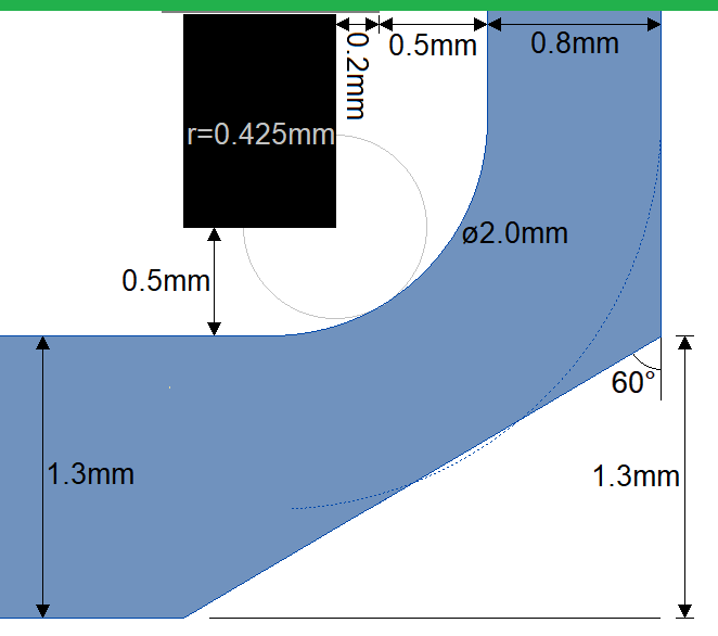
Mill the pallet edges, engraving, board pocket, component pockets and pallet openings. Component pockets are first cleared (roughed) with a flat-bottom end mill, after which a ball nose end mill is used to finish the pocket’s rounded edges.
-
Stop to flip the sheet left/right (around the y-axis, so that +x becomes -x). Use the same registration holes and pins.
-
Mill pressure relief areas (if any) and chamfer the leading/trailing pallet edges and the edges of pallet openings.
This requires several different types of carbide or diamond cutting tools, as shown in the following table:
-
Purpose
Style
Diameter (mm)
Stiffener/alignment holes
Drill/mill
3.0
Openings in pallet
Drill/mill
2.5
Engraved text and symbols
Drill/mill
1.0, 2.5
Board pocket edges
Flat bottom
2.5
Pocket floors and rail fingers
Flat bottom
6.0
Component pocket edges
Ball nose
2.0
Bottom side chamfered edges
120° chamfer cut
6.0
The 3.0 mm tool should have a length of cut (LOC) at least 10 mm longer than the sheet thickness. All other tools should have a length of cut (LOC) at least 2 mm longer than the sheet thickness.